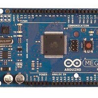
A000047 Arduino, A000047 Datasheet - Page 350
A000047
Manufacturer Part Number
A000047
Description
MCU, MPU & DSP Development Tools Mega2560
Manufacturer
Arduino
Series
-r
Type
MCUr
Specifications of A000047
Processor To Be Evaluated
ATmega2560
Interface Type
USB, I2C, SPI
Dimensions
4 in x 2.1 in
Operating Supply Voltage
5 V
Contents
Board
Lead Free Status / RoHS Status
Lead free / RoHS Compliant
For Use With/related Products
ATmega2560


29.8.1
29.8.2
2549M–AVR–09/10
Serial Programming Pin Mapping
Serial Programming Algorithm
Table 29-15. Pin Mapping Serial Programming
Figure 29-10. Serial Programming and Verify
Notes:
Depending on CKSEL Fuses, a valid clock must be present. The minimum low and high periods
for the serial clock (SCK) input are defined as follows:
Low: > 2 CPU clock cycles for f
High: > 2 CPU clock cycles for f
When writing serial data to the ATmega640/1280/1281/2560/2561, data is clocked on the rising
edge of SCK.
When reading data from the ATmega640/1280/1281/2560/2561, data is clocked on the falling
edge of SCK. See
Symbol
1. If the device is clocked by the internal Oscillator, it is no need to connect a clock source to the
2. V
PDO
SCK
PDI
XTAL1 pin.
programming the EEPROM, an auto-erase cycle is built into the self-timed programming oper-
ation (in the Serial mode ONLY) and there is no need to first execute the Chip Erase
instruction. The Chip Erase operation turns the content of every memory location in both the
Program and EEPROM arrays into 0xFF.
CC
- 0.3V < AVCC < V
Figure 29-12 on page 353
(TQFP-100)
Pins
PB2
PB3
PB1
PDO
SCK
PDI
ck
ck
CC
ATmega640/1280/1281/2560/2561
< 12 MHz, 3 CPU clock cycles for f
< 12 MHz, 3 CPU clock cycles for f
+ 0.3V, however, AVCC should always be within 1.8V - 5.5V.When
XT AL1
RESET
GND
(TQFP-64)
for timing details.
(1)
Pins
PE0
PE1
PB1
AVCC
VCC
+1.8V - 5.5V
+1.8V - 5.5V
I/O
O
I
I
(2)
ck
ck
>= 12 MHz
>= 12 MHz
Serial Data out
Serial Data in
Description
Serial Clock
350
Related parts for A000047
Image
Part Number
Description
Manufacturer
Datasheet
Request
R

Part Number:
Description:
Daughter Cards & OEM Boards ARDUINO UNO PROTO PCB REV 3
Manufacturer:
Arduino
Part Number:
Description:
Daughter Cards & OEM Boards ARDUINO SHIELD PROTO KIT REV 3
Manufacturer:
Arduino
Part Number:
Description:
Daughter Cards & OEM Boards ARDUINO MEGA PROTO KIT REV 3
Manufacturer:
Arduino
Part Number:
Description:
Daughter Cards & OEM Boards ARDUINO MEGA PROTO PCB REV 3
Manufacturer:
Arduino
Part Number:
Description:
Development Boards & Kits - AVR ARDUINO STARTER KIT W/ UNO REV3
Manufacturer:
Arduino
Part Number:
Description:
RF Development Tools ARDUINO SHIELD WIRELESS PROTO
Manufacturer:
Arduino
Datasheet:
Part Number:
Description:
RF Development Tools ARDUINO SHIELD WIRELESS WITH SD
Manufacturer:
Arduino
Datasheet:

Part Number:
Description:
Development Software Getting started w/Arduino
Manufacturer:
Arduino

Part Number:
Description:
Ethernet Modules & Development Tools Ethernet Shield for Arduino
Manufacturer:
Arduino

Part Number:
Description:
MCU, MPU & DSP Development Tools LilyPad Arduino Main Board
Manufacturer:
Arduino

Part Number:
Description:
ARDUINO NANO Board
Manufacturer:
Arduino
Datasheet:
Part Number:
Description:
Ethernet Modules & Development Tools ETHERNET SHEILD PoE FOR ARDUINO
Manufacturer:
Arduino
Datasheet:

Part Number:
Description:
ATMEGA328 MCU IC W/ Arduino UNO Bootloader
Manufacturer:
Arduino
Datasheet:
Part Number:
Description:
Memory Cards MICRO SD CARD 1GB WITH SD ADAPTER
Manufacturer:
Arduino