A000047 Arduino, A000047 Datasheet - Page 244
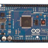
A000047
Manufacturer Part Number
A000047
Description
MCU, MPU & DSP Development Tools Mega2560
Manufacturer
Arduino
Series
-r
Type
MCUr
Specifications of A000047
Processor To Be Evaluated
ATmega2560
Interface Type
USB, I2C, SPI
Dimensions
4 in x 2.1 in
Operating Supply Voltage
5 V
Contents
Board
Lead Free Status / RoHS Status
Lead free / RoHS Compliant
For Use With/related Products
ATmega2560


23.3.4
23.3.5
Figure 23-6. Typical Data Transmission
2549M–AVR–09/10
SDA
SCL
START
Data Packet Format
Combining Address and Data Packets into a Transmission
Addr MSB
1
2
All data packets transmitted on the TWI bus are nine bits long, consisting of one data byte and
an acknowledge bit. During a data transfer, the Master generates the clock and the START and
STOP conditions, while the Receiver is responsible for acknowledging the reception. An
Acknowledge (ACK) is signalled by the Receiver pulling the SDA line low during the ninth SCL
cycle. If the Receiver leaves the SDA line high, a NACK is signalled. When the Receiver has
received the last byte, or for some reason cannot receive any more bytes, it should inform the
Transmitter by sending a NACK after the final byte. The MSB of the data byte is transmitted first.
Figure 23-5. Data Packet Format
A transmission basically consists of a START condition, a SLA+R/W, one or more data packets
and a STOP condition. An empty message, consisting of a START followed by a STOP condi-
tion, is illegal. Note that the Wired-ANDing of the SCL line can be used to implement
handshaking between the Master and the Slave. The Slave can extend the SCL low period by
pulling the SCL line low. This is useful if the clock speed set up by the Master is too fast for the
Slave, or the Slave needs extra time for processing between the data transmissions. The Slave
extending the SCL low period will not affect the SCL high period, which is determined by the
Master. As a consequence, the Slave can reduce the TWI data transfer speed by prolonging the
SCL duty cycle.
Figure 23-6
between the SLA+R/W and the STOP condition, depending on the software protocol imple-
mented by the application software.
SLA+R/W
Aggregate
Transmitter
SDA from
SDA from
SCL from
Receiver
Master
SDA
Addr LSB
SLA+R/W
7
shows a typical data transmission. Note that several data bytes can be transmitted
R/W
8
ACK
Data MSB
9
1
ATmega640/1280/1281/2560/2561
2
Data MSB
1
Data Byte
7
2
Data Byte
Data LSB
8
7
ACK
9
Data LSB
8
ACK
9
STOP, REPEATED
START or Next
Data Byte
STOP
244
Related parts for A000047
Image
Part Number
Description
Manufacturer
Datasheet
Request
R

Part Number:
Description:
Daughter Cards & OEM Boards ARDUINO UNO PROTO PCB REV 3
Manufacturer:
Arduino
Part Number:
Description:
Daughter Cards & OEM Boards ARDUINO SHIELD PROTO KIT REV 3
Manufacturer:
Arduino
Part Number:
Description:
Daughter Cards & OEM Boards ARDUINO MEGA PROTO KIT REV 3
Manufacturer:
Arduino
Part Number:
Description:
Daughter Cards & OEM Boards ARDUINO MEGA PROTO PCB REV 3
Manufacturer:
Arduino
Part Number:
Description:
Development Boards & Kits - AVR ARDUINO STARTER KIT W/ UNO REV3
Manufacturer:
Arduino
Part Number:
Description:
RF Development Tools ARDUINO SHIELD WIRELESS PROTO
Manufacturer:
Arduino
Datasheet:
Part Number:
Description:
RF Development Tools ARDUINO SHIELD WIRELESS WITH SD
Manufacturer:
Arduino
Datasheet:

Part Number:
Description:
Development Software Getting started w/Arduino
Manufacturer:
Arduino

Part Number:
Description:
Ethernet Modules & Development Tools Ethernet Shield for Arduino
Manufacturer:
Arduino

Part Number:
Description:
MCU, MPU & DSP Development Tools LilyPad Arduino Main Board
Manufacturer:
Arduino

Part Number:
Description:
ARDUINO NANO Board
Manufacturer:
Arduino
Datasheet:
Part Number:
Description:
Ethernet Modules & Development Tools ETHERNET SHEILD PoE FOR ARDUINO
Manufacturer:
Arduino
Datasheet:

Part Number:
Description:
ATMEGA328 MCU IC W/ Arduino UNO Bootloader
Manufacturer:
Arduino
Datasheet:
Part Number:
Description:
Memory Cards MICRO SD CARD 1GB WITH SD ADAPTER
Manufacturer:
Arduino