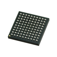
KSZ8893MBLI Micrel Inc, KSZ8893MBLI Datasheet - Page 24

KSZ8893MBLI
Manufacturer Part Number
KSZ8893MBLI
Description
2+1 Port 10/100 Switch W/ Tranceivers & Frame Buffers ( )
Manufacturer
Micrel Inc
Datasheet
1.KSZ8893MBLI.pdf
(116 pages)
Specifications of KSZ8893MBLI
Controller Type
Ethernet Switch Controller
Interface
MII, RMII, SNI
Voltage - Supply
3.1 V ~ 3.5 V
Operating Temperature
-40°C ~ 85°C
Mounting Type
Surface Mount
Package / Case
100-LFBGA
Number Of Primary Switch Ports
3
Operating Supply Voltage (typ)
3.3V
Fiber Support
Yes
Integrated Led Drivers
Yes
Power Supply Type
Analog/Digital
Data Rate (typ)
10/100Mbps
Vlan Support
Yes
Operating Temperature (max)
85C
Operating Temperature (min)
-40C
Mounting
Surface Mount
Jtag Support
No
Operating Supply Voltage (max)
3.5V
Operating Supply Voltage (min)
3.1V
Operating Temperature Classification
Industrial
Data Rate
100Mbps
Lead Free Status / RoHS Status
Lead free / RoHS Compliant
Current - Supply
-
Lead Free Status / RoHS Status
Not Compliant, Lead free / RoHS Compliant
Other names
576-3575
Available stocks
Company
Part Number
Manufacturer
Quantity
Price
Company:
Part Number:
KSZ8893MBLI
Manufacturer:
Micrel
Quantity:
2 022
February 2010
Ball Number
E9
E10
D9
D10
C5, D8, E8, H6,
H7
C4
Ball Number
Ball Name
PS1
PS0
TESTEN
SCANEN
VDDC
VDDCO
Ball Name
Type
I
I
Ipd
Ipd
P
P
Type
(1)
(1)
24
Ball Function Description
Serial bus configuration pins to select mode of access to
KSZ8893MBL internal registers.
[PS1, PS0] = [0, 0] — I
(If EEPROM is not detected, the KSZ8893MBL will be
configured with the default values of its internal registers and
the values of its strap-in pins.)
[PS1, PS0] = [0, 1] — I
The external I
The KSZ8893MBL device addresses are:
1011_1111
1011_1110
[PS1, PS0] = [1, 0] — SPI slave mode
[PS1, PS0] = [1, 1] – SMI-mode
In this mode, the KSZ8893MBL provides access to all its
internal 8-bit registers through its MDC and MDIO pins.
Note:
When (PS1, PS0) ≠ (1,1), the KSZ8893MBL provides access
to its 16-bit MIIM registers through its MDC and MDIO pins.
Scan Test Enable
For normal operation, pull-down this pin to ground.
Scan Test Scan Mux Enable
For normal operation, pull-down this pin to ground.
1.2V digital V
1.2V digital V
Provides V
(pin E3, F3 and G3), V
recommended the pin should be connected to 3.3V power rail
by a 100ohm resistor for the internal LDO application.
Ball Function Description
Interface Signals
SPIQ
SCL
SDA
SPIS_N
Interface Signals
SPIQ
SCL
SDA
SPIS_N
Interface Signals
SPIQ
SCL
SDA
SPIS_N
OUT_1V2
DD
DD
2
<write>
<read>
C master will drive the SCL clock.
to KSZ8893MBL’s input power pins: V
Type
O
O
I/O
I
Type
O
I
I/O
I
Type
O
I
I
I
DDC
2
2
C master (EEPROM) mode
C slave mode
(pins C5, D8, E8, H6 and H7). It is
Description
Not used (tri-stated)
I
I
Not used
Description
Not used (tri-stated)
I
I
Not used
Description
SPI data out
SPI clock
SPI data In
SPI chip select
2
2
2
2
C clock
C data I/O
C clock
C data I/O
M9999-021110-1.6
DDA


