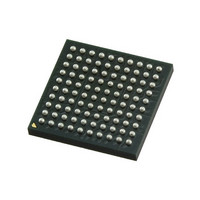
KSZ8893MBLI Micrel Inc, KSZ8893MBLI Datasheet - Page 52

KSZ8893MBLI
Manufacturer Part Number
KSZ8893MBLI
Description
2+1 Port 10/100 Switch W/ Tranceivers & Frame Buffers ( )
Manufacturer
Micrel Inc
Datasheet
1.KSZ8893MBLI.pdf
(116 pages)
Specifications of KSZ8893MBLI
Controller Type
Ethernet Switch Controller
Interface
MII, RMII, SNI
Voltage - Supply
3.1 V ~ 3.5 V
Operating Temperature
-40°C ~ 85°C
Mounting Type
Surface Mount
Package / Case
100-LFBGA
Number Of Primary Switch Ports
3
Operating Supply Voltage (typ)
3.3V
Fiber Support
Yes
Integrated Led Drivers
Yes
Power Supply Type
Analog/Digital
Data Rate (typ)
10/100Mbps
Vlan Support
Yes
Operating Temperature (max)
85C
Operating Temperature (min)
-40C
Mounting
Surface Mount
Jtag Support
No
Operating Supply Voltage (max)
3.5V
Operating Supply Voltage (min)
3.1V
Operating Temperature Classification
Industrial
Data Rate
100Mbps
Lead Free Status / RoHS Status
Lead free / RoHS Compliant
Current - Supply
-
Lead Free Status / RoHS Status
Not Compliant, Lead free / RoHS Compliant
Other names
576-3575
Available stocks
Company
Part Number
Manufacturer
Quantity
Price
Company:
Part Number:
KSZ8893MBLI
Manufacturer:
Micrel
Quantity:
2 022
The following is a sample procedure for programming the KSZ8893MQL/MBL using the SPI bus:
1. At the board level, connect the KSZ8893MQL/MBL pins as follows:
2. Enable SPI slave mode by setting the KSZ8893MQL/MBL strap-in pins PS[1:0] (pins 100 and 101,
3. Power up the board and assert reset to the KSZ8893MQL/MBL.
4. Configure the desired register settings in the KSZ8893MQL/MBL, using the SPI write or multiple write
5. Read back and verify the register settings in the KSZ8893MQL/MBL, using the SPI read or multiple read
6. Write a ‘1’ to the “Start Switch” bit to start the KSZ8893MQL/MBL with the programmed settings.
Note: The “Start Switch” bit cannot be set to ‘0’ to stop the switch after an ‘1’ is written to this bit. Thus, it is
recommended that all switch configuration settings are programmed before the “Start Switch” bit is set to ‘1’.
Some of the configuration settings, such as “Aging enable”, “Auto Negotiation Enable”, “Force Speed” and “Power
down” can be programmed after the switch has been started.
The following four figures illustrate the SPI data cycles for “Write”, “Read”, “Multiple Write” and “Multiple Read”.
The read data is registered out of SPIQ on the falling edge of SPIC, and the data input on SPID is registered on
the rising edge of SPIC.
February 2010
respectively) to “10”.
After reset, the “Start Switch” bit (register 1 bit [0]) is set to ‘0’.
command.
command.
KSZ8893MQL/MBL Pin #
99
97
98
96
SPIS_N
SPIQ
SPIC
SPID
X
0
0
WRITE COMMAND
0
Table 15. KSZ8893MQL/MBL SPI Connections
KSZ8893MQL/MBL Signal Name
SPIS_N
SCL
(SPIC)
SDA
(SPID)
SPIQ
0
0
Figure 8. SPI Write Data Cycle
0
1
0
A7 A6 A5 A4 A3 A2 A1 A0
52
WRITE ADDRESS
External Processor Signal Description
SPI Slave Select
SPI Clock
SPI Data
(Master output; Slave input)
SPI Data
(Master input; Slave output)
D7
D6
D5
WRITE DATA
D4
D3
M9999-021110-1.6
D2
D1
D0


