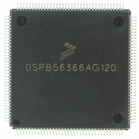
DSPB56366AG120 Freescale Semiconductor, DSPB56366AG120 Datasheet - Page 8

DSPB56366AG120
Manufacturer Part Number
DSPB56366AG120
Description
IC DSP 24BIT AUD 120MHZ 144-LQFP
Manufacturer
Freescale Semiconductor
Series
Symphony™r
Type
Audio Processorr
Datasheet
1.DSPB56366AG120.pdf
(110 pages)
Specifications of DSPB56366AG120
Interface
Host Interface, I²C, SAI, SPI
Clock Rate
120MHz
Non-volatile Memory
ROM (240 kB)
On-chip Ram
69kB
Voltage - I/o
3.30V
Voltage - Core
3.30V
Operating Temperature
-40°C ~ 110°C
Mounting Type
Surface Mount
Package / Case
144-LQFP
Lead Free Status / RoHS Status
Lead free / RoHS Compliant
Available stocks
Company
Part Number
Manufacturer
Quantity
Price
Company:
Part Number:
DSPB56366AG120
Manufacturer:
TOSHIBA
Quantity:
639
Company:
Part Number:
DSPB56366AG120
Manufacturer:
FREESCAL
Quantity:
273
Company:
Part Number:
DSPB56366AG120
Manufacturer:
Freescale Semiconductor
Quantity:
10 000
2.4
2.5
When the DSP56366 enters a low-power standby mode (stop or wait), it releases bus mastership and
tri-states the relevant port A signals: A0–A17, D0–D23, AA0/RAS0–AA2/RAS2, RD, WR, BB, CAS.
2-4
PINIT/NMI
Ground Name
Signal
EXTAL
Name
PCAP
GND
GND
GND
GND
D
C
S
Clock and PLL
External Memory Expansion Port (Port A)
H
(2)
(4)
(2)
Type
Input
Input
Input
Data Bus Ground—GND
must be tied externally to all other chip ground connections. The user must provide adequate external
decoupling capacitors. There are four GND
Bus Control Ground—GND
be tied externally to all other chip ground connections. The user must provide adequate external
decoupling capacitors. There are two GND
Host Ground—GND
externally to all other chip ground connections. The user must provide adequate external decoupling
capacitors. There is one GND
SHI, ESAI, ESAI_1, DAX and Timer Ground—GND
DAX and Timer. This connection must be tied externally to all other chip ground connections. The user
must provide adequate external decoupling capacitors. There are two GND
during
Reset
State
Input
Input
Input
External Clock Input—An external clock source must be connected to EXTAL in order
to supply the clock to the internal clock generator and PLL.
This input cannot tolerate 5 V.
PLL Capacitor—PCAP is an input connecting an off-chip capacitor to the PLL filter.
Connect one capacitor terminal to PCAP and the other terminal to V
If the PLL is not used, PCAP may be tied to V
PLL Initial/Nonmaskable Interrupt—During assertion of RESET, the value of
PINIT/NMI is written into the PLL Enable (PEN) bit of the PLL control register,
determining whether the PLL is enabled or disabled. After RESET de assertion and
during normal instruction processing, the PINIT/NMI Schmitt-trigger input is a
negative-edge-triggered nonmaskable interrupt (NMI) request internally synchronized
to internal system clock.
This input cannot tolerate 5 V.
h
Table 2-4 Clock and PLL Signals
is an isolated ground for the HD08 I/O drivers. This connection must be tied
Table 2-3 Grounds (continued)
DSP56366 Technical Data, Rev. 3.1
D
is an isolated ground for sections of the data bus I/O drivers. This connection
C
H
is an isolated ground for the bus control I/O drivers. This connection must
connection.
C
D
connections.
connections.
Description
Signal Description
S
is an isolated ground for the SHI, ESAI, ESAI_1,
CC
, GND, or left floating.
S
connections.
Freescale Semiconductor
CCP
.


