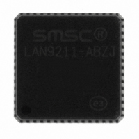
LAN9211-ABZJ SMSC, LAN9211-ABZJ Datasheet - Page 134

LAN9211-ABZJ
Manufacturer Part Number
LAN9211-ABZJ
Description
IC ETHERNET CTLR SGL CHIP 56-QFN
Manufacturer
SMSC
Type
Single Chip MAC and PHY Controllerr
Datasheet
1.LAN9211-ABZJ.pdf
(147 pages)
Specifications of LAN9211-ABZJ
Controller Type
Ethernet Controller
Interface
Serial EEPROM
Voltage - Supply
3.3V
Operating Temperature
0°C ~ 70°C
Mounting Type
Surface Mount
Package / Case
56-QFN
Product
Ethernet Controllers
Number Of Transceivers
1
Standard Supported
IEEE 802.3 or IEEE 802.3u
Data Rate
10 Mbps or 100 Mbps
Supply Voltage (max)
5 V
Supply Voltage (min)
3.3 V
Supply Current (max)
86 mA
Maximum Operating Temperature
+ 70 C
Ethernet Connection Type
100BASE-TX or 10BASE-T
Minimum Operating Temperature
0 C
Mounting Style
SMD/SMT
No. Of Ports
2
Ethernet Type
IEEE 802.3 / 802.3u
Interface Type
HBI
Supply Current
86mA
Supply Voltage Range
2.97V To 3.63V
Operating Temperature Range
0°C To +70°C
Rohs Compliant
Yes
Lead Free Status / RoHS Status
Lead free / RoHS Compliant
Current - Supply
-
Lead Free Status / Rohs Status
Lead free / RoHS Compliant
Other names
638-1049-6
Available stocks
Company
Part Number
Manufacturer
Quantity
Price
Company:
Part Number:
LAN9211-ABZJ
Manufacturer:
Standard
Quantity:
3
Part Number:
LAN9211-ABZJ
Manufacturer:
SMSC
Quantity:
20 000
Revision 2.7 (03-15-10)
6.7
SYMBOL
FIFO_SEL
nCS, nWR
Data Bus
t
cycle
t
t
t
t
t
t
csh
asu
dsu
A[2:1]
csl
ah
dh
In this mode the upper address inputs are not decoded, and any write to the LAN9211 will write the
TX Data FIFO. This mode is enabled when FIFO_SEL is driven high during a write access. This is
normally accomplished by connecting the FIFO_SEL signal to a high-order address line. This mode is
useful when the host processor must increment its address when accessing the LAN9211. Timing is
identical to a PIO write, and the FIFO_SEL signal has the same timing characteristics as the address
lines.
Note: The “Data Bus” width is 16 bits.
Note: A TX Data FIFO Direct PIO Write cycle begins when both nCS and nWR are asserted. The
TX Data FIFO Direct PIO Writes
DESCRIPTION
Write Cycle Time
nCS, nWR Assertion Time
nCS, nWR Deassertion Time
Address, FIFO_SEL Setup to nCS, nWR Assertion
Address, FIFO_SEL Hold Time
Data Setup to nCS, nWR Deassertion
Data Hold Time
cycle ends when either or both nCS and nWR are deasserted. They may be asserted and
deasserted in any order.
Figure 6.6 TX Data FIFO Direct PIO Write Timing
Table 6.8 TX Data FIFO Direct PIO Write Timing
DATASHEET
High-Performance Small Form Factor Single-Chip Ethernet Controller with HP Auto-MDIX Support
134
MIN
45
32
13
0
7
0
0
TYP
MAX
SMSC LAN9211
Datasheet
UNITS
ns
ns
ns
ns
ns
ns
ns


