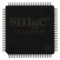
FDC37C669-MT SMSC, FDC37C669-MT Datasheet - Page 30

FDC37C669-MT
Manufacturer Part Number
FDC37C669-MT
Description
IC CTRLR SUPER I/O FLPPY 100TQFP
Manufacturer
SMSC
Datasheet
1.FDC37C669-MT.pdf
(162 pages)
Specifications of FDC37C669-MT
Controller Type
I/O Controller
Interface
ISA Host
Voltage - Supply
4.5 V ~ 5.5 V
Current - Supply
25mA
Operating Temperature
0°C ~ 70°C
Mounting Type
Surface Mount
Package / Case
100-TQFP, 100-VQFP
Lead Free Status / RoHS Status
Lead free / RoHS Compliant
Other names
638-1008
Available stocks
Company
Part Number
Manufacturer
Quantity
Price
Company:
Part Number:
FDC37C669-MT
Manufacturer:
Microchip Technology
Quantity:
10 000
- Current page: 30 of 162
- Download datasheet (619Kb)
DATA REGISTER (FIFO)
Address 3F5 READ/WRITE
All command parameter information, disk data and result
status are transferred between the host processor and
the floppy disk controller through the Data Register.
Data transfers are governed by the RQM and DIO bits in
the Main Status Register.
The Data Register defaults to FIFO disabled mode after
any form of reset.
compatibility. The default values can be changed through
the Configure command (enable full FIFO operation with
threshold control). The advantage of the FIFO is that it
allows the system a larger DMA latency without causing a
disk error. Table 15 gives several examples of the delays
with
*The 2 Mbps data rate is only available if V
This maintains PC/AT hardware
Table 13- FIFO Service Delay
FIFO THRESHOLD
FIFO THRESHOLD
EXAMPLES
FIFO THRESHOLD
EXAMPLES
15 bytes
2 bytes
8 bytes
1 byte
15 bytes
2 bytes
8 bytes
EXAMPLES
1 byte
15 bytes
2 bytes
8 bytes
1 byte
CC
= 5V.
1 x 8 µs - 1.5 µs = 6.5 µs
2 x 8 µs - 1.5 µs = 14.5 µs
8 x 8 µs - 1.5 µs = 62.5 µs
15 x 8 µs - 1.5 µs = 118.5 µs
1 x 16 µs - 1.5 µs = 14.5 µs
2 x 16 µs - 1.5 µs = 30.5 µs
8 x 16 µs - 1.5 µs = 126.5 µs
15 x 16 µs - 1.5 µs = 238.5 µs
MAXIMUM DELAY TO SERVICING AT
MAXIMUM DELAY TO SERVICING AT 1
a
1 x 4 µs - 1.5 µs = 2.5 µs
2 x 4 µs - 1.5 µs = 6.5 µs
8 x 4 µs - 1.5 µs = 30.5 µs
15 x 4 µs - 1.5 µs = 58.5 µs
SERVICING AT 2 Mbps* DATA
30
500 Kbps DATA RATE
MAXIMUM DELAY TO
FIFO. The data is based upon the following formula:
At the start of a command, the FIFO action is always
disabled and command parameters must be sent based
upon the RQM and DIO bit settings. As the command
execution phase is entered, the FIFO is cleared of any
data to ensure that invalid data is not transferred.
An overrun or underrun will terminate the current
command and the transfer of data. Disk writes will
complete the current sector by generating a 00 pattern
and valid CRC. Reads require the host to remove the
remaining data so that the result phase may be entered.
Threshold # x
Mbps DATA RATE
RATE
DATA RATE
1
-1.5 µs = DELAY
Related parts for FDC37C669-MT
Image
Part Number
Description
Manufacturer
Datasheet
Request
R

Part Number:
Description:
FAST ETHERNET PHYSICAL LAYER DEVICE
Manufacturer:
SMSC Corporation
Datasheet:

Part Number:
Description:
357-036-542-201 CARDEDGE 36POS DL .156 BLK LOPRO
Manufacturer:
SMSC Corporation
Datasheet:

Part Number:
Description:
357-036-542-201 CARDEDGE 36POS DL .156 BLK LOPRO
Manufacturer:
SMSC Corporation
Datasheet:

Part Number:
Description:
357-036-542-201 CARDEDGE 36POS DL .156 BLK LOPRO
Manufacturer:
SMSC Corporation
Datasheet:

Part Number:
Description:
4-PORT USB2.0 HUB CONTROLLER
Manufacturer:
SMSC Corporation
Datasheet:

Part Number:
Description:
Manufacturer:
SMSC Corporation
Datasheet:

Part Number:
Description:
Manufacturer:
SMSC Corporation
Datasheet:

Part Number:
Description:
FDC37C672ENHANCED SUPER I/O CONTROLLER WITH FAST IR
Manufacturer:
SMSC Corporation
Datasheet:

Part Number:
Description:
COM90C66LJPARCNET Controller/Transceiver with AT Interface and On-Chip RAM
Manufacturer:
SMSC Corporation
Datasheet:

Part Number:
Description:
Manufacturer:
SMSC Corporation
Datasheet:

Part Number:
Description:
Manufacturer:
SMSC Corporation
Datasheet:

Part Number:
Description:
Manufacturer:
SMSC Corporation
Datasheet:

Part Number:
Description:
Manufacturer:
SMSC Corporation
Datasheet:


