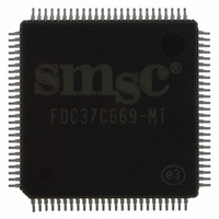
FDC37C669-MT SMSC, FDC37C669-MT Datasheet - Page 76

FDC37C669-MT
Manufacturer Part Number
FDC37C669-MT
Description
IC CTRLR SUPER I/O FLPPY 100TQFP
Manufacturer
SMSC
Datasheet
1.FDC37C669-MT.pdf
(162 pages)
Specifications of FDC37C669-MT
Controller Type
I/O Controller
Interface
ISA Host
Voltage - Supply
4.5 V ~ 5.5 V
Current - Supply
25mA
Operating Temperature
0°C ~ 70°C
Mounting Type
Surface Mount
Package / Case
100-TQFP, 100-VQFP
Lead Free Status / RoHS Status
Lead free / RoHS Compliant
Other names
638-1008
Available stocks
Company
Part Number
Manufacturer
Quantity
Price
Company:
Part Number:
FDC37C669-MT
Manufacturer:
Microchip Technology
Quantity:
10 000
- Current page: 76 of 162
- Download datasheet (619Kb)
LINE CONTROL REGISTER (LCR)
Address Offset = 3H, DLAB = 0, READ/WRITE
This register contains the format information of the serial
line. The bit definitions are:
Bits 0 and 1
These two bits specify the number of bits in each
transmitted or received serial character. The encoding of
bits 0 and 1 is as follows:
The Start, Stop and Parity bits are not included in the
word length.
Bit 2
This bit specifies the number of stop bits in each
transmitted or received serial character. The following
table summarizes the information.
Note: The receiver will ignore all stop bits beyond the
first, regardless of the number used in transmitting.
Bit 3
Parity Enable bit. When bit 3 is a logic "1", a parity bit
is generated (transmit data) or
BIT 2
0
1
1
1
1
BIT 1
WORD LENGTH
0
0
1
1
5 bits
6 bits
7 bits
8 bits
BIT 0 WORD LENGTH
--
0
1
0
1
5 Bits
6 Bits
7 Bits
8 Bits
NUMBER OF
STOP BITS
1.5
1
2
2
2
76
checked (receive data) between the last data word bit and
the first stop bit of the serial data. (The parity bit is used to
generate an even or odd number of 1s when the data
word bits and the parity bit are summed).
Bit 4
Even Parity Select bit. When bit 3 is a logic "1" and bit 4
is a logic "0", an odd number of logic "1"'s is transmitted
or checked in the data word bits and the parity bit. When
bit 3 is a logic "1" and bit 4 is a logic "1" an even number
of bits is transmitted and checked.
Bit 5
Stick Parity bit. When bit 3 is a logic "1" and bit 5 is a
logic "1", the parity bit is transmitted and then detected by
the receiver in the opposite state indicated by bit 4.
Bit 6
Set Break Control bit. When bit 6 is a logic "1", the
transmit data output (TXD) is forced to the Spacing or
logic "0" state and remains there (until reset by a low level
bit 6) regardless of other transmitter activity. This feature
enables the Serial Port to alert a terminal in a
communications system.
Bit 7
Divisor Latch Access bit (DLAB). It must be set high
(logic "1") to access the Divisor Latches of the Baud Rate
Generator during read or write operations. It must be set
low (logic "0") to access the Receiver Buffer Register, the
Transmitter Holding Register, or the Interrupt Enable
Register.
MODEM CONTROL REGISTER (MCR)
Address Offset = 4H, DLAB = X, READ/WRITE
This 8 bit register controls the interface with the MODEM
or data set (or device emulating a MODEM).
contents of the MODEM control register are described
below.
The
Related parts for FDC37C669-MT
Image
Part Number
Description
Manufacturer
Datasheet
Request
R

Part Number:
Description:
FAST ETHERNET PHYSICAL LAYER DEVICE
Manufacturer:
SMSC Corporation
Datasheet:

Part Number:
Description:
357-036-542-201 CARDEDGE 36POS DL .156 BLK LOPRO
Manufacturer:
SMSC Corporation
Datasheet:

Part Number:
Description:
357-036-542-201 CARDEDGE 36POS DL .156 BLK LOPRO
Manufacturer:
SMSC Corporation
Datasheet:

Part Number:
Description:
357-036-542-201 CARDEDGE 36POS DL .156 BLK LOPRO
Manufacturer:
SMSC Corporation
Datasheet:

Part Number:
Description:
4-PORT USB2.0 HUB CONTROLLER
Manufacturer:
SMSC Corporation
Datasheet:

Part Number:
Description:
Manufacturer:
SMSC Corporation
Datasheet:

Part Number:
Description:
Manufacturer:
SMSC Corporation
Datasheet:

Part Number:
Description:
FDC37C672ENHANCED SUPER I/O CONTROLLER WITH FAST IR
Manufacturer:
SMSC Corporation
Datasheet:

Part Number:
Description:
COM90C66LJPARCNET Controller/Transceiver with AT Interface and On-Chip RAM
Manufacturer:
SMSC Corporation
Datasheet:

Part Number:
Description:
Manufacturer:
SMSC Corporation
Datasheet:

Part Number:
Description:
Manufacturer:
SMSC Corporation
Datasheet:

Part Number:
Description:
Manufacturer:
SMSC Corporation
Datasheet:

Part Number:
Description:
Manufacturer:
SMSC Corporation
Datasheet:


