DS3170N+ Maxim Integrated Products, DS3170N+ Datasheet - Page 135
DS3170N+
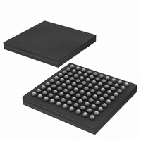
Manufacturer Part Number
DS3170N+
Description
IC TXRX DS3/E3 100-CSBGA
Manufacturer
Maxim Integrated Products
Datasheet
1.DS3170.pdf
(230 pages)
Specifications of DS3170N+
Function
Single-Chip Transceiver
Interface
DS3, E3
Number Of Circuits
1
Voltage - Supply
3.135 V ~ 3.465 V
Current - Supply
120mA
Operating Temperature
-40°C ~ 85°C
Mounting Type
Surface Mount
Package / Case
100-LBGA
Includes
DS3 Framers, E3 Framers, HDLC Controller, On-Chip BERTs
Lead Free Status / RoHS Status
Lead free / RoHS Compliant
Power (watts)
-


Bit 7: Transmit Manual Error Insert (TMEI) This bit is used to insert errors in all error insertion logic configured to
use this bit when PORT.CR1.MEIM=0. The error(s) will be inserted when this bit is toggled low to high.
Bit 6 : Transmit Manual Error Insert Mode (MEIM). These bits select the method transmit manual error insertion
for this port for error generators configured to use the external TMEI signal. The global updates are controlled by
the GL.CR1.MEIMS bit.
Bit 4: Performance Monitor Update Mode (PMUM). These bits select the method of updating the performance
monitor registers. The global updates are controlled by the GL.CR1.GPMU bits.
Bit 3: Performance Monitor Register Update (PMU) This bit is used to update all of the performance monitor
registers configured to use this bit when PORT.CR1.PMUM=0. The performance registers configured to use this
signal will be updated with the latest count value and the counters reset when this bit is toggled low to high. The bit
should remain high until the performance register update status bit (PORT.SR.PMS) goes high, then it should be
brought back low which clears the PMS status bit.
Bit 2: Power-Down (PD). When this bit is set, the LIU and digital logic for this port are powered down and
considered “out of service”. The logic is powered down by stopping the clocks. See the
section 10.3.
Bit 1: Reset Data Path (RSTDP). When this bit is set, it will force all of the internal data path registers to their
default state. This bit must be set high for a minimum of 100ns and then set back low. See the
Down
to one).
Bit 0: Reset (RST). When this bit is set, it will force all the internal data path and status and control registers
(except this RST bit) of this port to their default state. See the
be set high for a minimum of 100ns and then set back low. This software bit is logically OR’ed with the inverted
hardware signal RST and the GL.CR1.RST bit.
Register Name:
Register Description:
Register Address:
Bit #
Name
Default
Bit #
Name
Default
Bit 15: Transmit Line IO Signal Enable (TLEN). This bit is used to enable to transmit line interface output pins
TLCLK, TPOS/TDAT and TNEG.
Bit 14: Transmit LIU Tri-State (TTS) This bit is used to tri-state the transmit TXP and TXN pins. The LIU is still
powered up when the pins are tri-stated. It has no effect when the LIU is disabled and powered down.
section 10.3. Note: The Default State of this bit is 1 (after a general reset (port or global), this bit will be set
1 = Transmit BERT logic enabled
0 = Port software update via PORT.CR1.TMEI
1 = Global update source
0 = Port software update
1 = Global update
0 = Normal operation
1 = Power-down port circuits (default state)
0 = Normal operation
1 = Force all data path registers to their default values
0 = Normal operation
1 = Force all internal registers to their default values
0 = Disable, force outputs low
1 = Enable normal operation
RESERVED
TLEN
15
0
7
0
RESERVED
TTS
14
0
6
0
PORT.CR2
Port Control Register 2
042h
RMON
FM2
13
0
5
0
135 of 230
TLBO
FM1
12
0
4
0
Reset and Power-Down
RESERVED
FM0
11
0
3
0
DS3170 DS3/E3 Single-Chip Transceiver
RESERVED
LM2
10
0
2
0
section 10.3. This bit must
RESERVED
Reset and Power-Down
LM1
9
0
1
0
Reset and Power-
RESERVED
LM0
8
0
0
0
Related parts for DS3170N+
Image
Part Number
Description
Manufacturer
Datasheet
Request
R

Part Number:
Description:
IC TXRX DS3/E3 100-CSBGA
Manufacturer:
Maxim Integrated Products
Datasheet:

Part Number:
Description:
Network Controller & Processor ICs DS3-E3 Single-Chip T ransceiver T3-E3 Fra
Manufacturer:
Maxim Integrated Products
Datasheet:
Part Number:
Description:
MAX7528KCWPMaxim Integrated Products [CMOS Dual 8-Bit Buffered Multiplying DACs]
Manufacturer:
Maxim Integrated Products
Datasheet:
Part Number:
Description:
Single +5V, fully integrated, 1.25Gbps laser diode driver.
Manufacturer:
Maxim Integrated Products
Datasheet:
Part Number:
Description:
Single +5V, fully integrated, 155Mbps laser diode driver.
Manufacturer:
Maxim Integrated Products
Datasheet:
Part Number:
Description:
VRD11/VRD10, K8 Rev F 2/3/4-Phase PWM Controllers with Integrated Dual MOSFET Drivers
Manufacturer:
Maxim Integrated Products
Datasheet:
Part Number:
Description:
Highly Integrated Level 2 SMBus Battery Chargers
Manufacturer:
Maxim Integrated Products
Datasheet:
Part Number:
Description:
Current Monitor and Accumulator with Integrated Sense Resistor; ; Temperature Range: -40°C to +85°C
Manufacturer:
Maxim Integrated Products
Part Number:
Description:
TSSOP 14/A°/RS-485 Transceivers with Integrated 100O/120O Termination Resis
Manufacturer:
Maxim Integrated Products
Part Number:
Description:
TSSOP 14/A°/RS-485 Transceivers with Integrated 100O/120O Termination Resis
Manufacturer:
Maxim Integrated Products
Part Number:
Description:
QFN 16/A°/AC-DC and DC-DC Peak-Current-Mode Converters with Integrated Step
Manufacturer:
Maxim Integrated Products
Part Number:
Description:
TDFN/A/65V, 1A, 600KHZ, SYNCHRONOUS STEP-DOWN REGULATOR WITH INTEGRATED SWI
Manufacturer:
Maxim Integrated Products
Part Number:
Description:
Integrated Temperature Controller f
Manufacturer:
Maxim Integrated Products
Part Number:
Description:
SOT23-6/I°/45MHz to 650MHz, Integrated IF VCOs with Differential Output
Manufacturer:
Maxim Integrated Products
Part Number:
Description:
SOT23-6/I°/45MHz to 650MHz, Integrated IF VCOs with Differential Output
Manufacturer:
Maxim Integrated Products