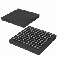
DS3170N+ Maxim Integrated Products, DS3170N+ Datasheet - Page 29

DS3170N+
Manufacturer Part Number
DS3170N+
Description
IC TXRX DS3/E3 100-CSBGA
Manufacturer
Maxim Integrated Products
Datasheet
1.DS3170.pdf
(230 pages)
Specifications of DS3170N+
Function
Single-Chip Transceiver
Interface
DS3, E3
Number Of Circuits
1
Voltage - Supply
3.135 V ~ 3.465 V
Current - Supply
120mA
Operating Temperature
-40°C ~ 85°C
Mounting Type
Surface Mount
Package / Case
100-LBGA
Includes
DS3 Framers, E3 Framers, HDLC Controller, On-Chip BERTs
Lead Free Status / RoHS Status
Lead free / RoHS Compliant
Power (watts)
-
- Current page: 29 of 230
- Download datasheet (3Mb)
RPOS /
RDAT
RNEG /
RLCV
TOH
TOHEN
PIN NAME
TYPE
Iad
Iad
I
I
Receive Positive AMI / Data
RPOS: When the port line is configured for B3ZS, HDB3 or AMI mode and the LIU is
disabled, a high on this pin indicates that a positive pulse has been detected using an
external LIU. The signal is sampled on the positive clock edge of the referenced clock
pin if the clock pin signal is not inverted, otherwise it is sampled on the falling edge of
the clock. The signal is typically referenced to the RLCLK line clock input pins, but it
can be referenced to the RCLKO output pins.
This input signal can be inverted.
RDAT: When the port line interface is configured for UNI mode, the un-encoded
receive signal is input on this pin. The signal is sampled on the positive clock edge of
the referenced clock pin if the clock pin signal is not inverted, otherwise it is sampled
on the falling edge of the clock. The signal is typically referenced to the RLCLK line
clock input pins, but it can be referenced to the RCLK output pins.
This input signal can be inverted.
o
o
Receive Negative AMI / Line Code Violation / Line OH Mask input
RNEG: When the port line is configured for B3ZS, HDB3 or AMI mode and the LIU is
disabled, a high on this pin indicates that a negative pulse has been detected using
an external LIU. The signal is sampled on the positive clock edge of the referenced
clock pin if the clock pin signal is not inverted, otherwise it is sampled on the falling
edge of the clock. The signal is typically referenced to the RLCLK line clock input
pins, but it can be referenced to the RCLKO output pins.
This input signal can be inverted.
o
o
RLCV: When the port line interface is configured for UNI mode, the BPV counter in
the encoder/decoder block is incremented each clock when this signal is high. The
signal is sampled on the positive clock edge of the referenced clock pin if the clock
pin signal is not inverted, otherwise it is sampled on the falling edge of the clock. The
signal is typically referenced to the RLCLK line clock input pins, but it can be
referenced to the RCLKO output pins.
This input signal can be inverted.
Transmit Overhead
TOH: When the port framer is configured for one of the DS3 or E3 framing modes,
this signal will be used to over-write the DS3 or E3 framing overhead bits when
TOHEN is active. In T3 mode, the X-bits, P-bits, M-bits, F-bits, and C-bits are input. In
G.751 E3 mode, all of the FAS, RAI, and National Use bits are input. In G.832 E3
mode, all of the FA1, FA2, EM, TR, MA, NR, and GC bytes are input. The TOHSOF
signal marks the start of the framing bit sequence. This signal is sampled at the same
time as the TOHCLK signal transitions high to low.
This signal can be inverted.
Transmit Overhead Enable / Start Of Frame Input
TOHEN: When the port framer is configured for one of the DS3 or E3 framing modes,
this signal will be used the determine which DS3 or E3 framing overhead bits to over-
write with the signal on the TOH pin. The TOHSOF signal marks the start of the
framing bit sequence. This signal is sampled at the same time as the TOHCLK signal
transitions high to low.
This signal can be inverted.
DS3: 44.736 Mbps +20ppm
E3: 34.368 Mbps +20ppm
DS3: 44.736 Mbps +20ppm
E3: 34.368 Mbps +20ppm
DS3/E3 Overhead Interface
29 of 230
PIN DESCRIPTION
DS3170 DS3/E3 Single-Chip Transceiver
Related parts for DS3170N+
Image
Part Number
Description
Manufacturer
Datasheet
Request
R

Part Number:
Description:
IC TXRX DS3/E3 100-CSBGA
Manufacturer:
Maxim Integrated Products
Datasheet:

Part Number:
Description:
Network Controller & Processor ICs DS3-E3 Single-Chip T ransceiver T3-E3 Fra
Manufacturer:
Maxim Integrated Products
Datasheet:

Part Number:
Description:
MAX7528KCWPMaxim Integrated Products [CMOS Dual 8-Bit Buffered Multiplying DACs]
Manufacturer:
Maxim Integrated Products
Datasheet:

Part Number:
Description:
Single +5V, fully integrated, 1.25Gbps laser diode driver.
Manufacturer:
Maxim Integrated Products
Datasheet:

Part Number:
Description:
Single +5V, fully integrated, 155Mbps laser diode driver.
Manufacturer:
Maxim Integrated Products
Datasheet:

Part Number:
Description:
VRD11/VRD10, K8 Rev F 2/3/4-Phase PWM Controllers with Integrated Dual MOSFET Drivers
Manufacturer:
Maxim Integrated Products
Datasheet:

Part Number:
Description:
Highly Integrated Level 2 SMBus Battery Chargers
Manufacturer:
Maxim Integrated Products
Datasheet:

Part Number:
Description:
Current Monitor and Accumulator with Integrated Sense Resistor; ; Temperature Range: -40°C to +85°C
Manufacturer:
Maxim Integrated Products

Part Number:
Description:
TSSOP 14/A°/RS-485 Transceivers with Integrated 100O/120O Termination Resis
Manufacturer:
Maxim Integrated Products

Part Number:
Description:
TSSOP 14/A°/RS-485 Transceivers with Integrated 100O/120O Termination Resis
Manufacturer:
Maxim Integrated Products

Part Number:
Description:
QFN 16/A°/AC-DC and DC-DC Peak-Current-Mode Converters with Integrated Step
Manufacturer:
Maxim Integrated Products

Part Number:
Description:
TDFN/A/65V, 1A, 600KHZ, SYNCHRONOUS STEP-DOWN REGULATOR WITH INTEGRATED SWI
Manufacturer:
Maxim Integrated Products

Part Number:
Description:
Integrated Temperature Controller f
Manufacturer:
Maxim Integrated Products

Part Number:
Description:
SOT23-6/I°/45MHz to 650MHz, Integrated IF VCOs with Differential Output
Manufacturer:
Maxim Integrated Products

Part Number:
Description:
SOT23-6/I°/45MHz to 650MHz, Integrated IF VCOs with Differential Output
Manufacturer:
Maxim Integrated Products


