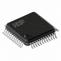
SC68C2550BIB48,151 NXP Semiconductors, SC68C2550BIB48,151 Datasheet - Page 10

SC68C2550BIB48,151
Manufacturer Part Number
SC68C2550BIB48,151
Description
IC UART DUAL W/FIFO 48-LQFP
Manufacturer
NXP Semiconductors
Type
5 V, 3.3 V and 2.5 V dual UART, 5 Mbit/s with 16-byte FIFOsr
Datasheet
1.SC68C2550BIB48151.pdf
(36 pages)
Specifications of SC68C2550BIB48,151
Number Of Channels
2, DUART
Package / Case
48-LQFP
Features
False-start Bit Detection
Fifo's
16 Byte
Voltage - Supply
2.5V, 3.3V, 5V
With Auto Flow Control
Yes
With False Start Bit Detection
Yes
With Modem Control
Yes
With Cmos
Yes
Mounting Type
Surface Mount
Data Rate
5 Mbps
Supply Voltage (max)
5.5 V
Supply Voltage (min)
2.25 V
Supply Current
4.5 mA
Maximum Operating Temperature
+ 85 C
Minimum Operating Temperature
- 40 C
Mounting Style
SMD/SMT
Operating Supply Voltage
2.5 V or 3.3 V or 5 V
Transmit Fifo
16Byte
Receive Fifo
16Byte
Transmitter And Receiver Fifo Counter
Yes
Package Type
LQFP
Operating Supply Voltage (max)
5.5V
Mounting
Surface Mount
Pin Count
48
Operating Temperature (min)
-40C
Operating Temperature (max)
85C
Operating Temperature Classification
Industrial
Lead Free Status / RoHS Status
Lead free / RoHS Compliant
Lead Free Status / RoHS Status
Lead free / RoHS Compliant, Lead free / RoHS Compliant
Other names
568-3296
935278765151
SC68C2550BIB48-S
935278765151
SC68C2550BIB48-S
Available stocks
Company
Part Number
Manufacturer
Quantity
Price
Company:
Part Number:
SC68C2550BIB48,151
Manufacturer:
NXP Semiconductors
Quantity:
10 000
NXP Semiconductors
SC68C2550B_3
Product data sheet
6.6 DMA operation
Table 6.
The SC68C2550B FIFO trigger level provides additional flexibility to the user for block
mode operation. LSR[6:5] provide an indication when the transmitter is empty or has an
empty location(s). The user can optionally operate the transmit and receive FIFOs in the
DMA mode (FCR[3]). When the transmit and receive FIFOs are enabled and the DMA
mode is de-activated (DMA Mode 0), the SC68C2550B activates the interrupt output pin
for each data transmit or receive operation. When DMA mode is activated (DMA Mode 1),
the user takes the advantage of block mode operation by loading or unloading the FIFO in
a block sequence determined by the receive trigger level and the transmit FIFO. In this
mode, the SC68C2550B sets the TXRDYn (or RXRDYn) output pin when characters in the
transmit FIFO is below 16, or the characters in the receive FIFOs are above the receive
trigger level.
Output
baud rate
50
75
110
150
300
600
1200
2400
3600
4800
7200
9600
19.2 k
38.4 k
57.6 k
115.2 k
Fig 3.
Crystal oscillator connection
Baud rate generator programming table using a 1.8432 MHz clock
Output
16 clock divisor
(decimal)
2304
1536
1047
768
384
192
96
48
32
24
16
12
6
3
2
1
5 V, 3.3 V and 2.5 V dual UART, 5 Mbit/s (max.), with 16-byte FIFOs
Rev. 03 — 9 October 2009
Output
16 clock divisor
(HEX)
900
600
417
300
180
C0
60
30
20
18
10
0C
06
03
02
01
XTAL1
1.8432 MHz
C1
22 pF
X1
XTAL2
002aab325
C2
33 pF
DLM
program value
(HEX)
09
06
04
03
01
00
00
00
00
00
00
00
00
00
00
00
SC68C2550B
© NXP B.V. 2009. All rights reserved.
DLL
program value
(HEX)
00
00
17
00
80
C0
60
30
20
18
10
0C
06
03
02
01
10 of 36


