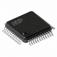
SC68C2550BIB48,151 NXP Semiconductors, SC68C2550BIB48,151 Datasheet - Page 21

SC68C2550BIB48,151
Manufacturer Part Number
SC68C2550BIB48,151
Description
IC UART DUAL W/FIFO 48-LQFP
Manufacturer
NXP Semiconductors
Type
5 V, 3.3 V and 2.5 V dual UART, 5 Mbit/s with 16-byte FIFOsr
Datasheet
1.SC68C2550BIB48151.pdf
(36 pages)
Specifications of SC68C2550BIB48,151
Number Of Channels
2, DUART
Package / Case
48-LQFP
Features
False-start Bit Detection
Fifo's
16 Byte
Voltage - Supply
2.5V, 3.3V, 5V
With Auto Flow Control
Yes
With False Start Bit Detection
Yes
With Modem Control
Yes
With Cmos
Yes
Mounting Type
Surface Mount
Data Rate
5 Mbps
Supply Voltage (max)
5.5 V
Supply Voltage (min)
2.25 V
Supply Current
4.5 mA
Maximum Operating Temperature
+ 85 C
Minimum Operating Temperature
- 40 C
Mounting Style
SMD/SMT
Operating Supply Voltage
2.5 V or 3.3 V or 5 V
Transmit Fifo
16Byte
Receive Fifo
16Byte
Transmitter And Receiver Fifo Counter
Yes
Package Type
LQFP
Operating Supply Voltage (max)
5.5V
Mounting
Surface Mount
Pin Count
48
Operating Temperature (min)
-40C
Operating Temperature (max)
85C
Operating Temperature Classification
Industrial
Lead Free Status / RoHS Status
Lead free / RoHS Compliant
Lead Free Status / RoHS Status
Lead free / RoHS Compliant, Lead free / RoHS Compliant
Other names
568-3296
935278765151
SC68C2550BIB48-S
935278765151
SC68C2550BIB48-S
Available stocks
Company
Part Number
Manufacturer
Quantity
Price
Company:
Part Number:
SC68C2550BIB48,151
Manufacturer:
NXP Semiconductors
Quantity:
10 000
NXP Semiconductors
SC68C2550B_3
Product data sheet
7.8 Modem Status Register (MSR)
This register provides the current state of the control interface signals from the modem, or
other peripheral device to which the SC68C2550B is connected. Four bits of this register
are used to indicate the changed information. These bits are set to a logic 1 whenever a
control input from the modem changes state. These bits are set to a logic 0 whenever the
CPU reads this register.
Table 19.
[1]
Bit
7
6
5
4
3
2
1
0
Whenever any MSR bit 0 to bit 3 is set to logic 1, a Modem Status Interrupt will be generated.
Symbol
MSR[7]
MSR[6]
MSR[5]
MSR[4]
MSR[3]
MSR[2]
MSR[1]
MSR[0]
Modem Status Register bits description
5 V, 3.3 V and 2.5 V dual UART, 5 Mbit/s (max.), with 16-byte FIFOs
Description
CD. During normal operation, this bit is the complement of the CDn input pin.
Reading this bit in the Loopback mode produces the state of MCR[3] (OP2).
RI. During normal operation, this bit is the complement of the RIn input pin.
Reading this bit in the Loopback mode produces the state of MCR[2] (OP1).
DSR. During normal operation, this bit is the complement of the DSRn input
pin. During the Loopback mode, this bit is equivalent to the state of MCR[0].
CTS. During normal operation, this bit is the complement of the CTSn input
pin. During the Loopback mode, this bit is equivalent to the state of MCR[1].
CD
RI
DSR
CTS
logic 0 = no change of state on CDn pin (normal default condition)
logic 1 = the CDn input pin to the SC68C2550B has changed state since
the last time it was read. A Modem Status Interrupt will be generated.
logic 0 = no change of state on RIn pin (normal default condition)
logic 1 = the RIn input pin to the SC68C2550B has changed from a logic 0
to a logic 1. A Modem Status Interrupt will be generated.
logic 0 = no change of state on DSRn pin (normal default condition)
logic 1 = the DSRn input pin to the SC68C2550B has changed state since
the last time it was read. A Modem Status Interrupt will be generated.
logic 0 = no change of state on CTSn pin (normal default condition)
logic 1 = the CTSn input pin to the SC68C2550B has changed state since
the last time it was read. A Modem Status Interrupt will be generated.
Rev. 03 — 9 October 2009
[1]
[1]
[1]
[1]
SC68C2550B
© NXP B.V. 2009. All rights reserved.
21 of 36


