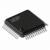
SC68C2550BIB48,151 NXP Semiconductors, SC68C2550BIB48,151 Datasheet - Page 11

SC68C2550BIB48,151
Manufacturer Part Number
SC68C2550BIB48,151
Description
IC UART DUAL W/FIFO 48-LQFP
Manufacturer
NXP Semiconductors
Type
5 V, 3.3 V and 2.5 V dual UART, 5 Mbit/s with 16-byte FIFOsr
Datasheet
1.SC68C2550BIB48151.pdf
(36 pages)
Specifications of SC68C2550BIB48,151
Number Of Channels
2, DUART
Package / Case
48-LQFP
Features
False-start Bit Detection
Fifo's
16 Byte
Voltage - Supply
2.5V, 3.3V, 5V
With Auto Flow Control
Yes
With False Start Bit Detection
Yes
With Modem Control
Yes
With Cmos
Yes
Mounting Type
Surface Mount
Data Rate
5 Mbps
Supply Voltage (max)
5.5 V
Supply Voltage (min)
2.25 V
Supply Current
4.5 mA
Maximum Operating Temperature
+ 85 C
Minimum Operating Temperature
- 40 C
Mounting Style
SMD/SMT
Operating Supply Voltage
2.5 V or 3.3 V or 5 V
Transmit Fifo
16Byte
Receive Fifo
16Byte
Transmitter And Receiver Fifo Counter
Yes
Package Type
LQFP
Operating Supply Voltage (max)
5.5V
Mounting
Surface Mount
Pin Count
48
Operating Temperature (min)
-40C
Operating Temperature (max)
85C
Operating Temperature Classification
Industrial
Lead Free Status / RoHS Status
Lead free / RoHS Compliant
Lead Free Status / RoHS Status
Lead free / RoHS Compliant, Lead free / RoHS Compliant
Other names
568-3296
935278765151
SC68C2550BIB48-S
935278765151
SC68C2550BIB48-S
Available stocks
Company
Part Number
Manufacturer
Quantity
Price
Company:
Part Number:
SC68C2550BIB48,151
Manufacturer:
NXP Semiconductors
Quantity:
10 000
NXP Semiconductors
SC68C2550B_3
Product data sheet
6.7 Loopback mode
The internal loopback capability allows on-board diagnostics. In the Loopback mode, the
normal modem interface pins are disconnected and reconfigured for loopback internally
(see
In the Loopback mode, the transmitter output pin (TXn) and the receiver input pin (RXn)
are disconnected from their associated interface pins, and instead are connected together
internally. The CTSn, DSRn, CDn, and RIn pins are disconnected from their normal
modem control inputs pins, and instead are connected internally to MCR[1] RTS, MCR[0]
DTR, MCR[3] (OP2) and MCR[2] (OP1). Loopback test data is entered into the transmit
holding register via the user data bus interface, D0 to D7. The transmit UART serializes
the data and passes the serial data to the receive UART via the internal loopback
connection. The receive UART converts the serial data back into parallel data that is then
made available at the user data interface D0 to D7. The user optionally compares the
received data to the initial transmitted data for verifying error-free operation of the UART
transmit/receive circuits.
In this mode, the receiver and transmitter interrupts are fully operational. The Modem
Control Interrupts are also operational.
Figure
4). MCR[3:0] register bits are used for controlling loopback diagnostic testing.
5 V, 3.3 V and 2.5 V dual UART, 5 Mbit/s (max.), with 16-byte FIFOs
Rev. 03 — 9 October 2009
SC68C2550B
© NXP B.V. 2009. All rights reserved.
11 of 36


