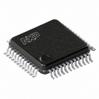
SC68C2550BIB48,151 NXP Semiconductors, SC68C2550BIB48,151 Datasheet - Page 6

SC68C2550BIB48,151
Manufacturer Part Number
SC68C2550BIB48,151
Description
IC UART DUAL W/FIFO 48-LQFP
Manufacturer
NXP Semiconductors
Type
5 V, 3.3 V and 2.5 V dual UART, 5 Mbit/s with 16-byte FIFOsr
Datasheet
1.SC68C2550BIB48151.pdf
(36 pages)
Specifications of SC68C2550BIB48,151
Number Of Channels
2, DUART
Package / Case
48-LQFP
Features
False-start Bit Detection
Fifo's
16 Byte
Voltage - Supply
2.5V, 3.3V, 5V
With Auto Flow Control
Yes
With False Start Bit Detection
Yes
With Modem Control
Yes
With Cmos
Yes
Mounting Type
Surface Mount
Data Rate
5 Mbps
Supply Voltage (max)
5.5 V
Supply Voltage (min)
2.25 V
Supply Current
4.5 mA
Maximum Operating Temperature
+ 85 C
Minimum Operating Temperature
- 40 C
Mounting Style
SMD/SMT
Operating Supply Voltage
2.5 V or 3.3 V or 5 V
Transmit Fifo
16Byte
Receive Fifo
16Byte
Transmitter And Receiver Fifo Counter
Yes
Package Type
LQFP
Operating Supply Voltage (max)
5.5V
Mounting
Surface Mount
Pin Count
48
Operating Temperature (min)
-40C
Operating Temperature (max)
85C
Operating Temperature Classification
Industrial
Lead Free Status / RoHS Status
Lead free / RoHS Compliant
Lead Free Status / RoHS Status
Lead free / RoHS Compliant, Lead free / RoHS Compliant
Other names
568-3296
935278765151
SC68C2550BIB48-S
935278765151
SC68C2550BIB48-S
Available stocks
Company
Part Number
Manufacturer
Quantity
Price
Company:
Part Number:
SC68C2550BIB48,151
Manufacturer:
NXP Semiconductors
Quantity:
10 000
NXP Semiconductors
Table 2.
SC68C2550B_3
Product data sheet
Symbol
RXRDYA
RXRDYB
TXA
TXB
TXRDYA
TXRDYB
V
XTAL1
XTAL2
n.c.
CC
Pin description
Pin
31
18
7
8
43
6
19, 42
13
14
12, 25,
29, 37
Type
O
O
O
O
O
O
I
I
O
-
…continued
Description
Receive Ready A, B (active LOW). These outputs provide the receive FIFO/RHR status for
individual receive channels (A-B). RXRDYn is primarily intended for monitoring DMA mode 1
transfers for the receive data FIFOs. A logic 0 indicates there is a receive data to
read/upload, that is, receive ready status with one or more receive characters available in
the FIFO/RHR. This pin is a logic 1 when the FIFO/RHR is empty or when the programmed
trigger level has not been reached. This signal can also be used for single mode transfers
(DMA mode 0).
Transmit data A, B. These outputs are associated with individual serial transmit channel
data from the SC68C2550B. The TXn pin will be a logic 1 during reset, idle (no data), or
when the transmitter is disabled. During the local Loopback mode, the TXn output pin is
disabled and transmit data is internally connected to the UART receive input.
Transmit Ready A, B (active LOW). These outputs provide the TX FIFO/THR status for
individual transmit channels (A-B). TXRDYn is primarily intended for monitoring DMA
mode 1 transfers for the transmit data FIFOs. An individual channel’s TXRDYA, TXRDYB
buffer ready status is indicated by logic 0, that is, at lease one location is empty and
available in the FIFO or THR. This pin goes to a logic 1 (DMA mode 1) when there are no
more empty locations in the FIFO or THR. This signal can also be used for single mode
transfers (DMA mode 0).
Power supply input
Crystal or external clock input. Functions as a crystal input or as an external clock input.
A crystal can be connected between this pin and XTAL2 to form an internal oscillator circuit.
Alternatively, an external clock can be connected to this pin to provide custom data rates.
(See
Output of the crystal oscillator or buffered clock. (See also XTAL1.) Crystal oscillator
output or buffered clock output. Should be left open if an external clock is connected to
XTAL1. For extended frequency operation, this pin should be tied to V
not connected
Section 6.5 “Programmable baud rate
5 V, 3.3 V and 2.5 V dual UART, 5 Mbit/s (max.), with 16-byte FIFOs
Rev. 03 — 9 October 2009
generator”.) See
Figure
SC68C2550B
3.
CC
© NXP B.V. 2009. All rights reserved.
via a 2 k resistor.
6 of 36


