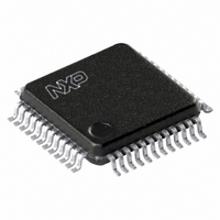
SC68C2550BIB48,151 NXP Semiconductors, SC68C2550BIB48,151 Datasheet - Page 24

SC68C2550BIB48,151
Manufacturer Part Number
SC68C2550BIB48,151
Description
IC UART DUAL W/FIFO 48-LQFP
Manufacturer
NXP Semiconductors
Type
5 V, 3.3 V and 2.5 V dual UART, 5 Mbit/s with 16-byte FIFOsr
Datasheet
1.SC68C2550BIB48151.pdf
(36 pages)
Specifications of SC68C2550BIB48,151
Number Of Channels
2, DUART
Package / Case
48-LQFP
Features
False-start Bit Detection
Fifo's
16 Byte
Voltage - Supply
2.5V, 3.3V, 5V
With Auto Flow Control
Yes
With False Start Bit Detection
Yes
With Modem Control
Yes
With Cmos
Yes
Mounting Type
Surface Mount
Data Rate
5 Mbps
Supply Voltage (max)
5.5 V
Supply Voltage (min)
2.25 V
Supply Current
4.5 mA
Maximum Operating Temperature
+ 85 C
Minimum Operating Temperature
- 40 C
Mounting Style
SMD/SMT
Operating Supply Voltage
2.5 V or 3.3 V or 5 V
Transmit Fifo
16Byte
Receive Fifo
16Byte
Transmitter And Receiver Fifo Counter
Yes
Package Type
LQFP
Operating Supply Voltage (max)
5.5V
Mounting
Surface Mount
Pin Count
48
Operating Temperature (min)
-40C
Operating Temperature (max)
85C
Operating Temperature Classification
Industrial
Lead Free Status / RoHS Status
Lead free / RoHS Compliant
Lead Free Status / RoHS Status
Lead free / RoHS Compliant, Lead free / RoHS Compliant
Other names
568-3296
935278765151
SC68C2550BIB48-S
935278765151
SC68C2550BIB48-S
Available stocks
Company
Part Number
Manufacturer
Quantity
Price
Company:
Part Number:
SC68C2550BIB48,151
Manufacturer:
NXP Semiconductors
Quantity:
10 000
NXP Semiconductors
10. Dynamic characteristics
Table 24.
T
[1]
[2]
[3]
[4]
SC68C2550B_3
Product data sheet
Symbol
t
t
t
t
t
t
t
t
t
t
t
t
t
t
t
t
t
t
t
t
t
t
f
t
t
t
t
d1
d2
d3
d4
d6
d7
d8
d9
d10
d11
d12
d13
d14
d15
d16
d17
d18
h2
h3
h4
WH
WL
XTAL
(RESET)
su1
su2
w(CS)
amb
RCLK is an internal signal derived from Divisor Latch LSB (DLL) and Divisor Latch MSB (DLM) divisor latches.
Applies to external clock; crystal oscillator maximum = 24 MHz.
Reset pulse must happen when CS is inactive.
f
= 40 C to +85 C; tolerance of V
XTAL
Parameter
R/W to chip select
read cycle delay
delay from CS to data
data disable time
write cycle delay
delay from write to output
delay to set interrupt from modem
input
delay to reset interrupt from read
delay from stop to set interrupt
delay from read to reset interrupt
delay from start to set interrupt
delay from write to transmit start
delay from write to reset interrupt
delay from stop to set RXRDY
delay from read to reset RXRDY
delay from write to set TXRDY
delay from start to reset TXRDY
R/W hold time from CS
data hold time
address hold time
pulse width HIGH
pulse width LOW
clock speed
RESET pulse width
address set-up time
data set-up time
CS pulse width
=
Dynamic characteristics
-------------- -
t
w clk
1
CC
10 %, unless specified otherwise.
5 V, 3.3 V and 2.5 V dual UART, 5 Mbit/s (max.), with 16-byte FIFOs
Conditions
25 pF load
25 pF load
25 pF load
25 pF load
25 pF load
25 pF load
25 pF load
Rev. 03 — 9 October 2009
[2][3]
[4]
8T
Min
RCLK
200
10
20
25
10
15
15
10
10
10
16
77
-
-
-
-
-
-
-
-
-
-
-
-
-
-
V
CC
[1]
= 2.5 V
24T
16T
1T
1T
Max
100
100
100
RCLK
100
100
100
RCLK
100
100
77
15
RCLK
RCLK
48
-
-
-
-
-
-
-
-
-
-
-
-
[1]
[1]
[1]
[1]
8T
SC68C2550B
V
CC
Min
RCLK
200
10
20
25
10
15
15
10
16
30
6
6
-
-
-
-
-
-
-
-
-
-
-
-
-
-
= 3.3 V and 5 V
[1]
© NXP B.V. 2009. All rights reserved.
24T
16T
1T
1T
Max
RCLK
100
RCLK
26
15
33
24
24
29
RCLK
70
75
70
RCLK
80
-
-
-
-
-
-
-
-
-
-
-
-
[1]
[1]
[1]
[1]
ns
ns
ns
ns
ns
ns
ns
ns
ns
ns
24 of 36
Unit
ns
ns
ns
ns
ns
ns
ns
ns
ns
ns
ns
ns
ns
ns
ns
MHz
ns


