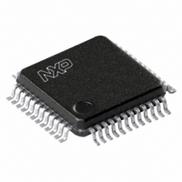
SC68C2550BIB48,151 NXP Semiconductors, SC68C2550BIB48,151 Datasheet - Page 15

SC68C2550BIB48,151
Manufacturer Part Number
SC68C2550BIB48,151
Description
IC UART DUAL W/FIFO 48-LQFP
Manufacturer
NXP Semiconductors
Type
5 V, 3.3 V and 2.5 V dual UART, 5 Mbit/s with 16-byte FIFOsr
Datasheet
1.SC68C2550BIB48151.pdf
(36 pages)
Specifications of SC68C2550BIB48,151
Number Of Channels
2, DUART
Package / Case
48-LQFP
Features
False-start Bit Detection
Fifo's
16 Byte
Voltage - Supply
2.5V, 3.3V, 5V
With Auto Flow Control
Yes
With False Start Bit Detection
Yes
With Modem Control
Yes
With Cmos
Yes
Mounting Type
Surface Mount
Data Rate
5 Mbps
Supply Voltage (max)
5.5 V
Supply Voltage (min)
2.25 V
Supply Current
4.5 mA
Maximum Operating Temperature
+ 85 C
Minimum Operating Temperature
- 40 C
Mounting Style
SMD/SMT
Operating Supply Voltage
2.5 V or 3.3 V or 5 V
Transmit Fifo
16Byte
Receive Fifo
16Byte
Transmitter And Receiver Fifo Counter
Yes
Package Type
LQFP
Operating Supply Voltage (max)
5.5V
Mounting
Surface Mount
Pin Count
48
Operating Temperature (min)
-40C
Operating Temperature (max)
85C
Operating Temperature Classification
Industrial
Lead Free Status / RoHS Status
Lead free / RoHS Compliant
Lead Free Status / RoHS Status
Lead free / RoHS Compliant, Lead free / RoHS Compliant
Other names
568-3296
935278765151
SC68C2550BIB48-S
935278765151
SC68C2550BIB48-S
Available stocks
Company
Part Number
Manufacturer
Quantity
Price
Company:
Part Number:
SC68C2550BIB48,151
Manufacturer:
NXP Semiconductors
Quantity:
10 000
NXP Semiconductors
SC68C2550B_3
Product data sheet
7.3.1.1 Mode 0 (FCR bit 3 = 0)
7.3.1.2 Mode 1 (FCR bit 3 = 1)
7.2.1 IER versus Transmit/Receive FIFO interrupt mode operation
7.2.2 IER versus Receive/Transmit FIFO polled mode operation
7.3.1 DMA mode
7.3 FIFO Control Register (FCR)
When the receive FIFO (FCR[0] = logic 1), and receive interrupts (IER[0] = logic 1) are
enabled, the receive interrupts and register status will reflect the following:
When FCR[0] = logic 1, resetting IER[3:0] enables the SC68C2550B in the FIFO polled
mode of operation. In this mode, interrupts are not generated and the user must poll the
LSR register for transmit and/or receive data status. Since the receiver and transmitter
have separate bits in the LSR either or both can be used in the polled mode by selecting
respective transmit or receive control bit(s).
This register is used to enable the FIFOs, clear the FIFOs, set the receive FIFO trigger
levels, and select the DMA mode.
Set and enable the interrupt for each single transmit or receive operation, and is similar to
the 68C450 mode. Transmit Ready pin (TXRDYn) will go to a logic 0 whenever the FIFO
(THR, if FIFO is not enabled) is empty. Receive Ready pin (RXRDYn) will go to a logic 0
whenever the Receive Holding Register (RHR) is loaded with a character.
Set and enable the interrupt in a block mode operation. The transmit interrupt is set when
the transmit FIFO is empty. TXRDYn pin remains a logic 0 as long as one empty FIFO
location is available. The receive interrupt is set when the receive FIFO fills to the
•
•
•
•
•
•
•
•
•
The receive RXRDY interrupt (Level 2 ISR interrupt) is issued to the external CPU
when the receive FIFO has reached the programmed trigger level. It will be cleared
when the receive FIFO drops below the programmed trigger level.
Receive FIFO status will also be reflected in the user accessible ISR register when
the receive FIFO trigger level is reached. Both the ISR register receive status bit and
the interrupt will be cleared when the FIFO drops below the trigger level.
The receive data ready bit (LSR[0]) is set as soon as a character is transferred from
the shift register (RSR) to the receive FIFO. It is reset when the FIFO is empty.
When the Transmit FIFO and interrupts are enabled, an interrupt is generated when
the transmit FIFO is empty due to the unloading of the data by the TSR and UART for
transmission via the transmission media. The interrupt is cleared either by reading the
ISR register, or by loading the THR with new data characters.
LSR[0] will be a logic 1 as long as there is one byte in the receive FIFO.
LSR[4:1] will provide the type of receive errors, or a receive break, if encountered.
LSR[5] will indicate when the transmit FIFO is empty.
LSR[6] will indicate when both the transmit FIFO and transmit shift register are empty.
LSR[7] will show if any FIFO data errors occurred.
5 V, 3.3 V and 2.5 V dual UART, 5 Mbit/s (max.), with 16-byte FIFOs
Rev. 03 — 9 October 2009
SC68C2550B
© NXP B.V. 2009. All rights reserved.
15 of 36


