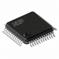
SC68C2550BIB48,151 NXP Semiconductors, SC68C2550BIB48,151 Datasheet - Page 18

SC68C2550BIB48,151
Manufacturer Part Number
SC68C2550BIB48,151
Description
IC UART DUAL W/FIFO 48-LQFP
Manufacturer
NXP Semiconductors
Type
5 V, 3.3 V and 2.5 V dual UART, 5 Mbit/s with 16-byte FIFOsr
Datasheet
1.SC68C2550BIB48151.pdf
(36 pages)
Specifications of SC68C2550BIB48,151
Number Of Channels
2, DUART
Package / Case
48-LQFP
Features
False-start Bit Detection
Fifo's
16 Byte
Voltage - Supply
2.5V, 3.3V, 5V
With Auto Flow Control
Yes
With False Start Bit Detection
Yes
With Modem Control
Yes
With Cmos
Yes
Mounting Type
Surface Mount
Data Rate
5 Mbps
Supply Voltage (max)
5.5 V
Supply Voltage (min)
2.25 V
Supply Current
4.5 mA
Maximum Operating Temperature
+ 85 C
Minimum Operating Temperature
- 40 C
Mounting Style
SMD/SMT
Operating Supply Voltage
2.5 V or 3.3 V or 5 V
Transmit Fifo
16Byte
Receive Fifo
16Byte
Transmitter And Receiver Fifo Counter
Yes
Package Type
LQFP
Operating Supply Voltage (max)
5.5V
Mounting
Surface Mount
Pin Count
48
Operating Temperature (min)
-40C
Operating Temperature (max)
85C
Operating Temperature Classification
Industrial
Lead Free Status / RoHS Status
Lead free / RoHS Compliant
Lead Free Status / RoHS Status
Lead free / RoHS Compliant, Lead free / RoHS Compliant
Other names
568-3296
935278765151
SC68C2550BIB48-S
935278765151
SC68C2550BIB48-S
Available stocks
Company
Part Number
Manufacturer
Quantity
Price
Company:
Part Number:
SC68C2550BIB48,151
Manufacturer:
NXP Semiconductors
Quantity:
10 000
NXP Semiconductors
SC68C2550B_3
Product data sheet
7.5 Line Control Register (LCR)
The Line Control Register is used to specify the asynchronous data communication
format. The word length, the number of stop bits, and the parity are selected by writing the
appropriate bits in this register.
Table 13.
Table 14.
Table 15.
Table 16.
Bit
7
6
5:3
2
1:0
LCR[5]
X
X
0
0
1
LCR[2]
0
1
1
LCR[1]
0
0
1
1
LCR[4]
X
0
1
0
1
Line Control Register bits description
LCR[5:3] parity selection
LCR[2] stop bit length
LCR[1:0] word length
Word length
5, 6, 7, 8
5
6, 7, 8
LCR[0]
0
1
0
1
Symbol
LCR[7]
LCR[6]
LCR[5:3]
LCR[2]
LCR[1:0]
5 V, 3.3 V and 2.5 V dual UART, 5 Mbit/s (max.), with 16-byte FIFOs
LCR[3]
0
1
1
1
1
Rev. 03 — 9 October 2009
Description
Divisor Latch enable. The internal baud rate counter latch and
Enhanced Feature mode enable.
Set break. When enabled, the Break control bit causes a break
condition to be transmitted (the TXn output is forced to a logic 0 state).
This condition exists until disabled by setting LCR[6] to a logic 0.
programs the parity conditions (see
Stop bits. The length of stop bit is specified by this bit in conjunction with
the programmed word length (see
Word length bits 1, 0. These two bits specify the word length to be
transmitted or received (see
logic 0 = Divisor Latch disabled (normal default condition).
Logic 1 = Divisor Latch enabled.
logic 0 = no break condition (normal default condition)
logic 1 = forces the transmitter output (TXn) to a logic 0 for alerting
the remote receiver to a line break condition
logic 0 or cleared = default condition
logic 0 or cleared = default condition
Parity selection
no parity
odd parity
even parity
forced parity ‘1’
forced parity ‘0’
Word length
5
6
7
8
Stop bit length (bit times)
1
1
2
1
2
Table
Table
16).
Table
15).
SC68C2550B
14)
© NXP B.V. 2009. All rights reserved.
18 of 36


