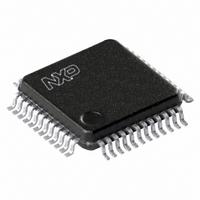
SC68C2550BIB48,151 NXP Semiconductors, SC68C2550BIB48,151 Datasheet - Page 8

SC68C2550BIB48,151
Manufacturer Part Number
SC68C2550BIB48,151
Description
IC UART DUAL W/FIFO 48-LQFP
Manufacturer
NXP Semiconductors
Type
5 V, 3.3 V and 2.5 V dual UART, 5 Mbit/s with 16-byte FIFOsr
Datasheet
1.SC68C2550BIB48151.pdf
(36 pages)
Specifications of SC68C2550BIB48,151
Number Of Channels
2, DUART
Package / Case
48-LQFP
Features
False-start Bit Detection
Fifo's
16 Byte
Voltage - Supply
2.5V, 3.3V, 5V
With Auto Flow Control
Yes
With False Start Bit Detection
Yes
With Modem Control
Yes
With Cmos
Yes
Mounting Type
Surface Mount
Data Rate
5 Mbps
Supply Voltage (max)
5.5 V
Supply Voltage (min)
2.25 V
Supply Current
4.5 mA
Maximum Operating Temperature
+ 85 C
Minimum Operating Temperature
- 40 C
Mounting Style
SMD/SMT
Operating Supply Voltage
2.5 V or 3.3 V or 5 V
Transmit Fifo
16Byte
Receive Fifo
16Byte
Transmitter And Receiver Fifo Counter
Yes
Package Type
LQFP
Operating Supply Voltage (max)
5.5V
Mounting
Surface Mount
Pin Count
48
Operating Temperature (min)
-40C
Operating Temperature (max)
85C
Operating Temperature Classification
Industrial
Lead Free Status / RoHS Status
Lead free / RoHS Compliant
Lead Free Status / RoHS Status
Lead free / RoHS Compliant, Lead free / RoHS Compliant
Other names
568-3296
935278765151
SC68C2550BIB48-S
935278765151
SC68C2550BIB48-S
Available stocks
Company
Part Number
Manufacturer
Quantity
Price
Company:
Part Number:
SC68C2550BIB48,151
Manufacturer:
NXP Semiconductors
Quantity:
10 000
NXP Semiconductors
SC68C2550B_3
Product data sheet
6.2 Internal registers
6.3 FIFO operation
The SC68C2550B provides two sets of internal registers (A and B) consisting of
12 registers each for monitoring and controlling the functions of each channel of the
UART. These registers are shown in
registers (THR/RHR), interrupt status and control registers (IER/ISR), a FIFO control
register (FCR), line status and control registers (LCR/LSR), modem status and control
registers (MCR/MSR), programmable data rate (clock) control registers (DLL/DLM), and a
user accessible scratchpad register (SPR).
Table 4.
[1]
[2]
The 16 byte transmit and receive data FIFOs are enabled by the FIFO Control Register
(FCR) bit 0. The user can set the receive trigger level via FCR[7:6], but not the transmit
trigger level. The receiver FIFO section includes a time-out function to ensure data is
delivered to the external CPU. An interrupt is generated whenever the Receive Holding
Register (RHR) has not been read following the loading of a character or the receive
trigger level has not been reached.
Table 5.
A2
General register set (THR/RHR, IER/ISR, MCR/MSR, FCR, LCR/LSR, SPR)
0
0
0
0
1
1
1
1
Baud rate register set (DLL/DLM)
0
0
Selected trigger level (characters)
1
4
8
14
These registers are accessible only when LCR[7] is a logic 0.
These registers are accessible only when LCR[7] is a logic 1.
A1
0
0
1
1
0
0
1
1
0
0
Internal registers decoding
Flow control mechanism
A0
0
1
0
1
0
1
0
1
0
1
5 V, 3.3 V and 2.5 V dual UART, 5 Mbit/s (max.), with 16-byte FIFOs
Read mode
Receive Holding Register
Interrupt Enable Register
Interrupt Status Register
Line Control Register
Modem Control Register
Line Status Register
Modem Status Register
Scratchpad Register
LSB of Divisor Latch
MSB of Divisor Latch
Rev. 03 — 9 October 2009
[2]
Table
IRQ pin activation
1
4
8
14
4. The UART registers function as data holding
Write mode
Transmit Holding Register
Interrupt Enable Register
FIFO Control Register
Line Control Register
Modem Control Register
n/a
n/a
Scratchpad Register
LSB of Divisor Latch
MSB of Divisor Latch
SC68C2550B
[1]
© NXP B.V. 2009. All rights reserved.
8 of 36


