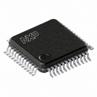
SC68C2550BIB48,151 NXP Semiconductors, SC68C2550BIB48,151 Datasheet - Page 16

SC68C2550BIB48,151
Manufacturer Part Number
SC68C2550BIB48,151
Description
IC UART DUAL W/FIFO 48-LQFP
Manufacturer
NXP Semiconductors
Type
5 V, 3.3 V and 2.5 V dual UART, 5 Mbit/s with 16-byte FIFOsr
Datasheet
1.SC68C2550BIB48151.pdf
(36 pages)
Specifications of SC68C2550BIB48,151
Number Of Channels
2, DUART
Package / Case
48-LQFP
Features
False-start Bit Detection
Fifo's
16 Byte
Voltage - Supply
2.5V, 3.3V, 5V
With Auto Flow Control
Yes
With False Start Bit Detection
Yes
With Modem Control
Yes
With Cmos
Yes
Mounting Type
Surface Mount
Data Rate
5 Mbps
Supply Voltage (max)
5.5 V
Supply Voltage (min)
2.25 V
Supply Current
4.5 mA
Maximum Operating Temperature
+ 85 C
Minimum Operating Temperature
- 40 C
Mounting Style
SMD/SMT
Operating Supply Voltage
2.5 V or 3.3 V or 5 V
Transmit Fifo
16Byte
Receive Fifo
16Byte
Transmitter And Receiver Fifo Counter
Yes
Package Type
LQFP
Operating Supply Voltage (max)
5.5V
Mounting
Surface Mount
Pin Count
48
Operating Temperature (min)
-40C
Operating Temperature (max)
85C
Operating Temperature Classification
Industrial
Lead Free Status / RoHS Status
Lead free / RoHS Compliant
Lead Free Status / RoHS Status
Lead free / RoHS Compliant, Lead free / RoHS Compliant
Other names
568-3296
935278765151
SC68C2550BIB48-S
935278765151
SC68C2550BIB48-S
Available stocks
Company
Part Number
Manufacturer
Quantity
Price
Company:
Part Number:
SC68C2550BIB48,151
Manufacturer:
NXP Semiconductors
Quantity:
10 000
NXP Semiconductors
SC68C2550B_3
Product data sheet
7.3.2 FIFO mode
programmed trigger level. However, the FIFO continues to fill regardless of the
programmed level until the FIFO is full. RXRDYn pin packages transitions LOW when the
FIFO reaches the trigger level, and transitions HIGH when the FIFO empties.
Table 9.
Bit
7:6
5:4
3
2
1
Symbol
FCR[7:6] RCVR trigger. These bits are used to set the trigger level for the receive FIFO
FCR[5:4] not used; initialized to logic 0
FCR[3]
FCR[2]
FCR[1]
FIFO Control Register bits description
Description
interrupt.
An interrupt is generated when the number of characters in the FIFO equals the
programmed trigger level. However, the FIFO will continue to be loaded until it
is full. Refer to
DMA mode select
Transmit operation in mode ‘0’: When the SC68C2550B is in the 68C450
mode (FIFOs disabled; FCR[0] = logic 0) or in the FIFO mode (FIFOs enabled;
FCR[0] = logic 1; FCR[3] = logic 0), and when there are no characters in the
transmit FIFO or transmit holding register, the TXRDYn pin will be a logic 0.
Once active, the TXRDYn pin will go to a logic 1 after the first character is
loaded into the transmit holding register.
Receive operation in mode ‘0’: When the SC68C2550B is in mode ‘0’
(FCR[0] = logic 0), or in the FIFO mode (FCR[3] = logic 0) and there is at least
one character in the receive FIFO, the RXRDYn pin will be a logic 0. Once
active, the RXRDYn pin will go to a logic 1 when there are no more characters
in the receiver.
Transmit operation in mode ‘1’: When the SC68C2550B is in FIFO mode
(FCR[0] = logic 1; FCR[3] = logic 1), the TXRDYn pin will be a logic 1 when the
transmit FIFO is completely full. It will be a logic 0 if one or more FIFO locations
are empty.
Receive operation in mode ‘1’: When the SC68C2550B is in FIFO mode
(FCR[0] = logic 1; FCR[3] = logic 1) and the trigger level has been reached, or a
Receive Time-Out has occurred, the RXRDYn pin will go to a logic 0. Once
activated, it will go to a logic 1 after there are no more characters in the FIFO.
XMIT FIFO reset
RCVR FIFO reset
5 V, 3.3 V and 2.5 V dual UART, 5 Mbit/s (max.), with 16-byte FIFOs
logic 0 (or cleared) = normal default condition
logic 1 = receive trigger level
logic 0 = set DMA mode ‘0’
logic 1 = set DMA mode ‘1’
logic 0 = transmit FIFO not reset (normal default condition)
logic 1 = clears the contents of the transmit FIFO and resets the FIFO
counter logic (the transmit shift register is not cleared or altered). This bit will
return to a logic 0 after clearing the FIFO.
logic 0 = receive FIFO not reset (normal default condition)
logic 1 = clears the contents of the receive FIFO and resets the FIFO counter
logic (the receive shift register is not cleared or altered). This bit will return to
a logic 0 after clearing the FIFO.
Rev. 03 — 9 October 2009
Table
10.
SC68C2550B
© NXP B.V. 2009. All rights reserved.
16 of 36


