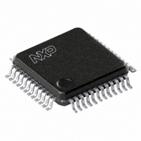
SC68C2550BIB48,151 NXP Semiconductors, SC68C2550BIB48,151 Datasheet - Page 4

SC68C2550BIB48,151
Manufacturer Part Number
SC68C2550BIB48,151
Description
IC UART DUAL W/FIFO 48-LQFP
Manufacturer
NXP Semiconductors
Type
5 V, 3.3 V and 2.5 V dual UART, 5 Mbit/s with 16-byte FIFOsr
Datasheet
1.SC68C2550BIB48151.pdf
(36 pages)
Specifications of SC68C2550BIB48,151
Number Of Channels
2, DUART
Package / Case
48-LQFP
Features
False-start Bit Detection
Fifo's
16 Byte
Voltage - Supply
2.5V, 3.3V, 5V
With Auto Flow Control
Yes
With False Start Bit Detection
Yes
With Modem Control
Yes
With Cmos
Yes
Mounting Type
Surface Mount
Data Rate
5 Mbps
Supply Voltage (max)
5.5 V
Supply Voltage (min)
2.25 V
Supply Current
4.5 mA
Maximum Operating Temperature
+ 85 C
Minimum Operating Temperature
- 40 C
Mounting Style
SMD/SMT
Operating Supply Voltage
2.5 V or 3.3 V or 5 V
Transmit Fifo
16Byte
Receive Fifo
16Byte
Transmitter And Receiver Fifo Counter
Yes
Package Type
LQFP
Operating Supply Voltage (max)
5.5V
Mounting
Surface Mount
Pin Count
48
Operating Temperature (min)
-40C
Operating Temperature (max)
85C
Operating Temperature Classification
Industrial
Lead Free Status / RoHS Status
Lead free / RoHS Compliant
Lead Free Status / RoHS Status
Lead free / RoHS Compliant, Lead free / RoHS Compliant
Other names
568-3296
935278765151
SC68C2550BIB48-S
935278765151
SC68C2550BIB48-S
Available stocks
Company
Part Number
Manufacturer
Quantity
Price
Company:
Part Number:
SC68C2550BIB48,151
Manufacturer:
NXP Semiconductors
Quantity:
10 000
NXP Semiconductors
5. Pinning information
Table 2.
SC68C2550B_3
Product data sheet
Symbol
A0
A1
A2
A3
CDA
CDB
CS
CTSA
CTSB
Pin description
Pin
28
27
26
11
40
16
10
38
23
5.1 Pinning
5.2 Pin description
Type
I
I
I
I
I
I
I
I
I
Fig 2.
Description
Address 0 select bit. Internal register address selection.
Address 1 select bit. Internal register address selection.
Address 2 select bit. Internal register address selection.
Address 3. A3 is used to select Channel A or Channel B. A logic LOW selects Channel A,
and a logic HIGH selects Channel B. (See
Carrier Detect (active LOW). These inputs are associated with individual UART channels A
through B. A logic 0 on this pin indicates that a carrier has been detected by the modem for
that channel.
Chip Select (active LOW). This pin enables data transfers between the user CPU and the
SC68C2550B for the channel(s) addressed. Individual UART sections (A, B) are addressed
by A3. See
Clear to Send (active LOW). These inputs are associated with individual UART channels, A
through B. A logic 0 on the CTSn pin indicates the modem or data set is ready to accept
transmit data from the SC68C2550B. Status can be tested by reading MSR[4]. This pin has
no effect on the UART’s transmit or receive operation.
Pin configuration for LQFP48
TXRDYB
Table
OP2B
5 V, 3.3 V and 2.5 V dual UART, 5 Mbit/s (max.), with 16-byte FIFOs
RXB
RXA
TXA
TXB
n.c.
CS
D5
D6
D7
A3
3.
Rev. 03 — 9 October 2009
10
11
12
1
2
3
4
5
6
7
8
9
SC68C2550BIB48
Table
3.)
SC68C2550B
002aab335
36
35
34
33
32
31
30
29
28
27
26
25
RESET
DTRB
DTRA
RTSA
OP2A
RXRDYA
IRQ
n.c.
A0
A1
A2
n.c.
© NXP B.V. 2009. All rights reserved.
4 of 36


