CRD4525-Q1 Cirrus Logic Inc, CRD4525-Q1 Datasheet - Page 26
CRD4525-Q1
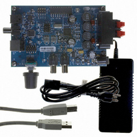
Manufacturer Part Number
CRD4525-Q1
Description
REFERENCE BOARD FOR CS4525 PWM
Manufacturer
Cirrus Logic Inc
Series
Popguard®r
Specifications of CRD4525-Q1
Amplifier Type
Class D
Output Type
2-Channel (Stereo)
Max Output Power X Channels @ Load
15W x 2 @ 8 Ohm
Voltage - Supply
12 V ~ 18 V
Operating Temperature
0°C ~ 70°C
Board Type
Fully Populated
Utilized Ic / Part
CS4525
Lead Free Status / RoHS Status
Contains lead / RoHS non-compliant
Other names
598-1586


26
6. APPLICATIONS
6.1
6.1.1
Software Mode
Maximum device flexibility and features are available when the CS4525 is used in software mode. The avail-
able features are described in the following sections. All device configuration is achieved via the I²C control
port as described in the
6.1.1.1
If an input clock is detected on the SYS_CLK pin following the release of RST, the device will automatically
use the SYS_CLK input as its clock source. The applied SYS_CLK clock signal must oscillate within the
frequency ranges specified in the SYS_CLK switching specifications table on
should be connected to ground and XTO should be left unconnected.
Figure 12
System Clocking
In software mode, the CS4525 can be clocked by a stable external clock source input on the SYS_CLK
pin or by a clock internally generated through the use of its internal oscillator driver circuit in conjunction
with an external crystal oscillator. The device automatically selects which of these clocks to use within
10 ms of the release of RST.
The internal clock is used to synchronize the input serial audio signals with the internal clock domain and
to clock the internal digital processing, sample-rate converter, and PWM modulators. It is also used to de-
termine the sample rate of the serial audio input signals in order to automatically configure the various
internal filter coefficients.
To ensure proper operation, the CS4525 must be informed of the nominal frequency of the supplied
SYS_CLK signal or the attached crystal via the ClkFreq[1:0] bits in the Clock Config register. These bits
must be set to the appropriate value before the PDnAll bit is cleared to initiate a power-up sequence. See
the
input frequency range specifications.
WARNING: The system clock source must never be removed or stopped while any of the power output
stages are powered-up (the PDnAll bit and any of the PDnOut1, PDnOut2, or PDnOut3/4 bits are cleared)
and connected to a load. Doing so may result in permanent damage to the CS4525 and connected trans-
ducers.
Referenced Control
ClkFreq[1:0].........................
PDnAll .................................
PDnOutX .............................
SYS_CLK Switching Specifications
below demonstrates a typical clocking configuration using the SYS_CLK input.
SYS_CLK Input Clock Mode
Clock
Figure 12. Typical SYS_CLK Input Clocking Configuration
I²C Control Port Description and Timing
Register Location
“Clock Frequency (ClkFreq[1:0])” on page 69
“Power Down (PDnAll)” on page 89
“Power Down PWM Power Output X (PDnOutX)” on page 89
Clock_In
DSP
and
Reset_Out
XTI Switching Specifications
RST
section on
SYS_CLK
CS4525
tables on
page
page
64.
XTO
XTI
page 23
23. In this mode, XTI
for complete
CS4525
DS726PP3
Related parts for CRD4525-Q1
Image
Part Number
Description
Manufacturer
Datasheet
Request
R

Part Number:
Description:
Development Kit
Manufacturer:
Cirrus Logic Inc
Datasheet:
Part Number:
Description:
Development Kit
Manufacturer:
Cirrus Logic Inc
Datasheet:


Part Number:
Description:
High-efficiency PFC + Fluorescent Lamp Driver Reference Design
Manufacturer:
Cirrus Logic Inc
Datasheet:
Part Number:
Description:
Development Kit
Manufacturer:
Cirrus Logic Inc
Datasheet:
Part Number:
Description:
Development Kit
Manufacturer:
Cirrus Logic Inc
Datasheet:

Part Number:
Description:
Development Kit
Manufacturer:
Cirrus Logic Inc
Datasheet:
Part Number:
Description:
Development Kit
Manufacturer:
Cirrus Logic Inc
Datasheet:
Part Number:
Description:
Development Kit
Manufacturer:
Cirrus Logic Inc
Datasheet:
Part Number:
Description:
Audio Modules & Development Tools EvalBd 30W Qd Hlf- Brdg Dig Amp Pwr Stg
Manufacturer:
Cirrus Logic Inc
Datasheet:

Part Number:
Description:
EVALUATION BOARD FOR CS8427
Manufacturer:
Cirrus Logic Inc
Datasheet:

Part Number:
Description:
BOARD EVAL FOR CS8416 RCVR
Manufacturer:
Cirrus Logic Inc
Datasheet:

Part Number:
Description:
EVALUATION BOARD FOR CS8420
Manufacturer:
Cirrus Logic Inc
Datasheet:

Part Number:
Description:
KIT DEVELOPMENT EP9315 ARM9
Manufacturer:
Cirrus Logic Inc
Datasheet: