CRD4525-Q1 Cirrus Logic Inc, CRD4525-Q1 Datasheet - Page 64
CRD4525-Q1
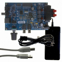
Manufacturer Part Number
CRD4525-Q1
Description
REFERENCE BOARD FOR CS4525 PWM
Manufacturer
Cirrus Logic Inc
Series
Popguard®r
Specifications of CRD4525-Q1
Amplifier Type
Class D
Output Type
2-Channel (Stereo)
Max Output Power X Channels @ Load
15W x 2 @ 8 Ohm
Voltage - Supply
12 V ~ 18 V
Operating Temperature
0°C ~ 70°C
Board Type
Fully Populated
Utilized Ic / Part
CS4525
Lead Free Status / RoHS Status
Contains lead / RoHS non-compliant
Other names
598-1586


64
6.8
I²C Control Port Description and Timing
The control port is used to access the registers allowing the CS4525 to be configured for the desired oper-
ational modes and formats. The operation of the control port may be completely asynchronous with respect
to the audio sample serial port. However, to avoid potential interference problems, the control port pins
should remain static if no operation is required. The control port operates in I²C Mode, with the CS4525 act-
ing as a slave device.
SDA is a bidirectional data line. Data is clocked into and out of the part by the clock, SCL. A 47 kΩ pull-up
or pull-down on the AUX_LRCK/AD0 pin will set AD0, the least significant bit of the device address. A pull-
up to VD will set AD0 to ‘1’ and a pull-down to DGND will set AD0 to ‘0’. The state of AUX_LRCK/AD0 is
sensed, and AD0 is set upon the release of RESET.
The signal timings for a read and write cycle are shown in
fined as a falling transition of SDA while the clock is high. A Stop condition is a rising transition while the
clock is high. All other transitions of SDA occur while the clock is low. The first byte sent to the CS4525 after
a Start condition consists of a 7 bit device address field and a R/W bit (high for a read, low for a write). The
upper 6 bits of the 7-bit address field are fixed at 100101. To communicate with a CS4525, the device ad-
dress field, which is the first byte sent to the CS4525, should match 100101 followed by the setting of AD0.
The eighth bit of the address is the R/W bit. If the operation is a write, the next byte is the memory address
pointer (MAP) which selects the register to be read or written. If the operation is a read, the contents of the
register pointed to by the MAP will be output. Setting the auto increment bit in MAP allows successive reads
or writes of consecutive registers. Each byte is separated by an acknowledge bit. The ACK bit is output from
the CS4525 after each input byte is read, and is input to the CS4525 from the microcontroller after each
transmitted byte.
Since the read operation can not set the MAP, an aborted write operation is used as a preamble. As shown
in
dition. The following pseudocode illustrates an aborted write operation followed by a read operation.
Send start condition.
Send 100101x0 (device address and write operation).
Receive acknowledge bit.
Send MAP byte, auto increment off.
Receive acknowledge bit.
Send stop condition, aborting write. (Optional.)
Send start condition.
Send 100101x1(device address and read operation).
SCL
SDA
Figure
SDA
SCL
START
34, the write operation is aborted after the acknowledge for the MAP byte by sending a stop con-
0
START
1
CHIP ADDRESS (WRITE)
1
0
0
0
1
2
CHIP ADDRESS (WRITE)
1
3
1
0
0 1 AD0 0
0
4
2
1
5
3
0
6
4
1
7
5
ACK
AD0
8
6
Figure 34. Control Port Timing, I²C Read
Figure 33. Control Port Timing, I²C Write
9
INCR
7
0
10 11
6
ACK
8
5
INCR
MAP BYTE
9
12 13 14 15
4
10 11
6
3
MAP BYTE
5
2
12
4
1
13 14 15
3
16
0
ACK
2
STOP
17 18
START
1
16 17 18
0
19
ACK
1
Figure 33
20 21 22 23 24
CHIP ADDRESS (READ)
0
7
0
19
6
DATA
1
0
24 25
1
1 AD0 1
0
and
ACK
25
26
26 27 28
Figure
27 28
7
ACK
DATA +1
6
7
DATA
34. A Start condition is de-
1
0
0
ACK
DATA +1
7
7
DATA +n
6
0
1
DATA + n
7
0
ACK
CS4525
DS726PP3
STOP
0
ACK
NO
STOP
Related parts for CRD4525-Q1
Image
Part Number
Description
Manufacturer
Datasheet
Request
R

Part Number:
Description:
Development Kit
Manufacturer:
Cirrus Logic Inc
Datasheet:
Part Number:
Description:
Development Kit
Manufacturer:
Cirrus Logic Inc
Datasheet:


Part Number:
Description:
High-efficiency PFC + Fluorescent Lamp Driver Reference Design
Manufacturer:
Cirrus Logic Inc
Datasheet:
Part Number:
Description:
Development Kit
Manufacturer:
Cirrus Logic Inc
Datasheet:
Part Number:
Description:
Development Kit
Manufacturer:
Cirrus Logic Inc
Datasheet:

Part Number:
Description:
Development Kit
Manufacturer:
Cirrus Logic Inc
Datasheet:
Part Number:
Description:
Development Kit
Manufacturer:
Cirrus Logic Inc
Datasheet:
Part Number:
Description:
Development Kit
Manufacturer:
Cirrus Logic Inc
Datasheet:
Part Number:
Description:
Audio Modules & Development Tools EvalBd 30W Qd Hlf- Brdg Dig Amp Pwr Stg
Manufacturer:
Cirrus Logic Inc
Datasheet:

Part Number:
Description:
EVALUATION BOARD FOR CS8427
Manufacturer:
Cirrus Logic Inc
Datasheet:

Part Number:
Description:
BOARD EVAL FOR CS8416 RCVR
Manufacturer:
Cirrus Logic Inc
Datasheet:

Part Number:
Description:
EVALUATION BOARD FOR CS8420
Manufacturer:
Cirrus Logic Inc
Datasheet:

Part Number:
Description:
KIT DEVELOPMENT EP9315 ARM9
Manufacturer:
Cirrus Logic Inc
Datasheet: