MC56F8367EVME Freescale Semiconductor, MC56F8367EVME Datasheet - Page 119
MC56F8367EVME
Manufacturer Part Number
MC56F8367EVME
Description
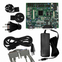
EVAL BOARD FOR MC56F83X
Manufacturer
Freescale Semiconductor
Type
DSPr
Specifications of MC56F8367EVME
Contents
Module and Misc Hardware
Processor To Be Evaluated
MC56F8145-67 and MC56F8345-67
Data Bus Width
16 bit
Interface Type
RS-232
Silicon Manufacturer
Freescale
Core Architecture
56800/E
Core Sub-architecture
56800/E
Silicon Core Number
MC56F
Silicon Family Name
MC56F83xx
Rohs Compliant
Yes
For Use With/related Products
MC56F83x5, MC56F83x6, MC56F83x7
Lead Free Status / RoHS Status
Lead free / RoHS Compliant


The upper four bits of the GPIOB register can function as GPIO, [A23:20], or as additional clock output
signals. GPIO has priority and is enabled/disabled via the GPIOB_PER. If GPIOB[7:4] are programmed
to operate as peripheral outputs, then the choice between [A23:20] and additional clock outputs is done
here in the CLKOSR. The default state is for the peripheral function of GPIOB[7:4] to be programmed as
[A23:20]. This can be changed by altering [A23:20] as shown in
6.5.7.1
This bit field is reserved or not implemented. It is read as 0 and cannot be modified by writing.
6.5.7.2
6.5.7.3
6.5.7.4
6.5.7.5
6.5.7.6
6.5.7.7
Selects clock to be muxed out on the CLKO pin.
Freescale Semiconductor
Preliminary
•
•
•
•
•
•
•
•
•
•
•
•
•
•
Base + $A
RESET
0 = Peripheral output function of GPIOB7 is defined to be A23
1 = Peripheral output function of GPIOB7 is defined to be the oscillator_clock (MSTR_OSC in
0 = Peripheral output function of GPIOB6 is defined to be A22
1 = Peripheral output function of GPIOB6 is defined to be SYS_CLK2
0 = Peripheral output function of GPIOB5 is defined to be A21
1 = Peripheral output function of GPIOB5 is defined to be SYS_CLK
0 = Peripheral output function of GPIOB4 is defined to be A20
1 = Peripheral output function of GPIOB4 is defined to be the prescaler_clock (FREF in
0 = CLKOUT output is enabled and will output the signal indicated by CLKOSEL
1 = CLKOUT is tri-stated
00000 = SYS_CLK (from OCCS - DEFAULT)
00001 = Reserved for factory test—56800E clock
00010 = Reserved for factory test—XRAM clock
00011 = Reserved for factory test—PFLASH odd clock
Read
Write
Reserved—Bits 15–10
Alternate GPIOB Peripheral Function for A23 (A23)—Bit 9
Alternate GPIOB Peripheral Function for A22 (A22)—Bit 8
Alternate GPIOB Peripheral Function for A21 (A21)—Bit 7
Alternate GPIOB Peripheral Function fpr A20 (A20)—Bit 6
Clockout Disable (CLKDIS)—Bit 5
CLockout Select (CLKOSEL)—Bits 4–0
15
0
0
14
0
0
Figure 6-9 CLKO Select Register (SIM_CLKOSR)
13
0
0
12
0
0
56F8367 Technical Data, Rev. 8
11
0
0
10
0
0
A23
9
0
A22
8
0
A21
7
0
Figure
A20
6
0
CLK
DIS
5
1
6-9.
4
0
3
0
CLKOSEL
2
0
Figure
Register Descriptions
1
0
Figure
3-4)
0
0
3-4)
119
Related parts for MC56F8367EVME
Image
Part Number
Description
Manufacturer
Datasheet
Request
R

Part Number:
Description:
56f8300 16-bit Digital Signal Controllers
Manufacturer:
Freescale Semiconductor, Inc
Datasheet:
Part Number:
Description:
Manufacturer:
Freescale Semiconductor, Inc
Datasheet:
Part Number:
Description:
Manufacturer:
Freescale Semiconductor, Inc
Datasheet:
Part Number:
Description:
Manufacturer:
Freescale Semiconductor, Inc
Datasheet:
Part Number:
Description:
Manufacturer:
Freescale Semiconductor, Inc
Datasheet:
Part Number:
Description:
Manufacturer:
Freescale Semiconductor, Inc
Datasheet:
Part Number:
Description:
Manufacturer:
Freescale Semiconductor, Inc
Datasheet:
Part Number:
Description:
Manufacturer:
Freescale Semiconductor, Inc
Datasheet:
Part Number:
Description:
Manufacturer:
Freescale Semiconductor, Inc
Datasheet:
Part Number:
Description:
Manufacturer:
Freescale Semiconductor, Inc
Datasheet:
Part Number:
Description:
Manufacturer:
Freescale Semiconductor, Inc
Datasheet:
Part Number:
Description:
Manufacturer:
Freescale Semiconductor, Inc
Datasheet:
Part Number:
Description:
Manufacturer:
Freescale Semiconductor, Inc
Datasheet:
Part Number:
Description:
Manufacturer:
Freescale Semiconductor, Inc
Datasheet:
Part Number:
Description:
Manufacturer:
Freescale Semiconductor, Inc
Datasheet: