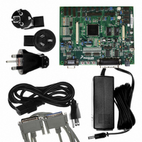
MC56F8367EVME Freescale Semiconductor, MC56F8367EVME Datasheet - Page 42

MC56F8367EVME
Manufacturer Part Number
MC56F8367EVME
Description
EVAL BOARD FOR MC56F83X
Manufacturer
Freescale Semiconductor
Type
DSPr
Specifications of MC56F8367EVME
Contents
Module and Misc Hardware
Processor To Be Evaluated
MC56F8145-67 and MC56F8345-67
Data Bus Width
16 bit
Interface Type
RS-232
Silicon Manufacturer
Freescale
Core Architecture
56800/E
Core Sub-architecture
56800/E
Silicon Core Number
MC56F
Silicon Family Name
MC56F83xx
Rohs Compliant
Yes
For Use With/related Products
MC56F83x5, MC56F83x6, MC56F83x7
Lead Free Status / RoHS Status
Lead free / RoHS Compliant
- Current page: 42 of 184
- Download datasheet (6Mb)
4.2 Program Map
The operating mode control bits (MA and MB) in the Operating Mode Register (OMR) control the
Program memory map. At reset, these bits are set as indicated in
map configurations that are possible at reset. After reset, the OMR MA bit can be changed and will have
an effect on the P-space memory map, as shown in
effect.
The device’s external memory interface (EMI) can operate much like the 56F80x family’s EMI, or it can
be operated in a mode similar to that used on other products in the 56800E family. Initially, CS0 and CS1
are configured as PS and DS, in a mode compatible with earlier 56800 devices.
Eighteen address lines are required to shadow the first 192K of internal program space when booting
externally for development purposes. Therefore, the entire complement of on-chip memory cannot be
accessed using a 16-bit 56800-compatible address bus. To address this situation, the EMI_MODE pin can
be used to configure four GPIO pins as Address[19:16] upon reset (Software reconfiguration of the highest
address lines [A20-23] is required if the full address range is to be used.)
The EMI_MODE bit also affects the reset vector address, as provided in
be configured as address or chip select signals to access addresses at P: $10 0000 and above.
Note: Program RAM is NOT available on the 56F8167 device.
42
1. This bit is only configured at reset. If the Flash secured state changes, this will not be reflected in MB until the next reset.
2. Changing MB in software will not affect Flash memory security.
Flash Secured
OMR MB =
OMR MA
State
0
1
0
0
1
1
1, 2
Table 4-3 Changing OMR MA Value During Normal Operation
Use internal P-space memory map configuration
Use external P-space memory map configuration – If MB = 0 at reset, changing this bit has no effect.
EXTBOOT Pin
OMR MA =
0
1
0
1
Table 4-2 OMR MB/MA Value at Reset
Mode 0 – Internal Boot; EMI is configured to use 16 address lines; Flash Memory is
secured; external P-space is not allowed; the EOnCE is disabled
Not valid; cannot boot externally if the Flash is secured and will actually configure to
00 state
Mode 0 – Internal Boot; EMI is configured to use 16 address lines
Mode 1 – External Boot; Flash Memory is not secured; EMI configuration is
determined by the state of the EMI_MODE pin
56F8367 Technical Data, Rev. 8
Chip Operating Mode
Table
Chip Operating Mode
4-3. Changing the OMR MB bit will have no
Table
4-2.
Table
Table 4-4
4-4. Additional pins must
Freescale Semiconductor
shows the memory
Preliminary
Related parts for MC56F8367EVME
Image
Part Number
Description
Manufacturer
Datasheet
Request
R
Part Number:
Description:
56f8300 16-bit Digital Signal Controllers
Manufacturer:
Freescale Semiconductor, Inc
Datasheet:
Part Number:
Description:
Manufacturer:
Freescale Semiconductor, Inc
Datasheet:
Part Number:
Description:
Manufacturer:
Freescale Semiconductor, Inc
Datasheet:
Part Number:
Description:
Manufacturer:
Freescale Semiconductor, Inc
Datasheet:
Part Number:
Description:
Manufacturer:
Freescale Semiconductor, Inc
Datasheet:
Part Number:
Description:
Manufacturer:
Freescale Semiconductor, Inc
Datasheet:
Part Number:
Description:
Manufacturer:
Freescale Semiconductor, Inc
Datasheet:
Part Number:
Description:
Manufacturer:
Freescale Semiconductor, Inc
Datasheet:
Part Number:
Description:
Manufacturer:
Freescale Semiconductor, Inc
Datasheet:
Part Number:
Description:
Manufacturer:
Freescale Semiconductor, Inc
Datasheet:
Part Number:
Description:
Manufacturer:
Freescale Semiconductor, Inc
Datasheet:
Part Number:
Description:
Manufacturer:
Freescale Semiconductor, Inc
Datasheet:
Part Number:
Description:
Manufacturer:
Freescale Semiconductor, Inc
Datasheet:
Part Number:
Description:
Manufacturer:
Freescale Semiconductor, Inc
Datasheet:
Part Number:
Description:
Manufacturer:
Freescale Semiconductor, Inc
Datasheet:


