MC56F8367EVME Freescale Semiconductor, MC56F8367EVME Datasheet - Page 129
MC56F8367EVME
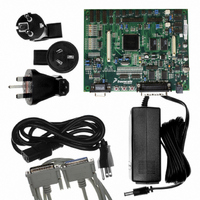
Manufacturer Part Number
MC56F8367EVME
Description
EVAL BOARD FOR MC56F83X
Manufacturer
Freescale Semiconductor
Type
DSPr
Specifications of MC56F8367EVME
Contents
Module and Misc Hardware
Processor To Be Evaluated
MC56F8145-67 and MC56F8345-67
Data Bus Width
16 bit
Interface Type
RS-232
Silicon Manufacturer
Freescale
Core Architecture
56800/E
Core Sub-architecture
56800/E
Silicon Core Number
MC56F
Silicon Family Name
MC56F83xx
Rohs Compliant
Yes
For Use With/related Products
MC56F83x5, MC56F83x6, MC56F83x7
Lead Free Status / RoHS Status
Lead free / RoHS Compliant


Resets
The 56800E core contains both STOP and WAIT instructions. Both put the CPU to sleep. For lowest
power consumption in Stop mode, the PLL can be shut down. This must be done explicitly before entering
Stop mode, since there is no automatic mechanism for this. When the PLL is shut down, the 56800E
system clock must be set equal to the oscillator output.
Some applications require the 56800E STOP/WAIT instructions be disabled. To disable those
instructions, write to the SIM control register (SIM_CONTROL) described in
Part
6.5.1. This procedure
can be on either a permanent or temporary basis. Permanently assigned applications last only until their
next reset.
6.9 Resets
The SIM supports four sources of reset. The two asynchronous sources are the external reset pin and the
Power-On Reset (POR). The two synchronous sources are the software reset, which is generated within
the SIM itself by writting to the SIM_CONTROL register, and the COP reset.
Reset begins with the assertion of any of the reset sources. Release of reset to various blocks is sequenced
21
to permit proper operation of the device. A POR reset is first extended for 2
clock cycles to permit
stabilization of the clock source, followed by a 32 clock window in which SIM clocking is initiated. It is
then followed by a 32 clock window in which peripherals are released to implement Flash security, and,
finally, followed by a 32 clock window in which the core is initialized. After completion of the described
reset sequence, application code will begin execution.
Resets may be asserted asynchronously, but are always released internally on a rising edge of the system
clock.
Part 7 Security Features
The 56F8367/56F8167 offer security features intended to prevent unauthorized users from reading the
contents of the Flash Memory (FM) array. The Flash security consists of several hardware interlocks that
block the means by which an unauthorized user could gain access to the Flash array.
However, part of the security must lie with the user’s code. An extreme example would be user’s code that
dumps the contents of the internal program, as this code would defeat the purpose of security. At the same
time, the user may also wish to put a “backdoor” in his program. As an example, the user downloads a
security key through the SCI, allowing access to a programming routine that updates parameters stored in
another section of the Flash.
7.1 Operation with Security Enabled
Once the user has programmed the Flash with his application code, the device can be secured by
programming the security bytes located in the FM configuration field, which occupies a portion of the FM
array. These non-volatile bytes will keep the part secured through reset and through power-down of the
device. Only two bytes within this field are used to enable or disable security. Refer to the Flash Memory
section in the 56F8300 Peripheral User Manual for the state of the security bytes and the resulting state
56F8367 Technical Data, Rev. 8
Freescale Semiconductor
129
Preliminary
Related parts for MC56F8367EVME
Image
Part Number
Description
Manufacturer
Datasheet
Request
R

Part Number:
Description:
56f8300 16-bit Digital Signal Controllers
Manufacturer:
Freescale Semiconductor, Inc
Datasheet:
Part Number:
Description:
Manufacturer:
Freescale Semiconductor, Inc
Datasheet:
Part Number:
Description:
Manufacturer:
Freescale Semiconductor, Inc
Datasheet:
Part Number:
Description:
Manufacturer:
Freescale Semiconductor, Inc
Datasheet:
Part Number:
Description:
Manufacturer:
Freescale Semiconductor, Inc
Datasheet:
Part Number:
Description:
Manufacturer:
Freescale Semiconductor, Inc
Datasheet:
Part Number:
Description:
Manufacturer:
Freescale Semiconductor, Inc
Datasheet:
Part Number:
Description:
Manufacturer:
Freescale Semiconductor, Inc
Datasheet:
Part Number:
Description:
Manufacturer:
Freescale Semiconductor, Inc
Datasheet:
Part Number:
Description:
Manufacturer:
Freescale Semiconductor, Inc
Datasheet:
Part Number:
Description:
Manufacturer:
Freescale Semiconductor, Inc
Datasheet:
Part Number:
Description:
Manufacturer:
Freescale Semiconductor, Inc
Datasheet:
Part Number:
Description:
Manufacturer:
Freescale Semiconductor, Inc
Datasheet:
Part Number:
Description:
Manufacturer:
Freescale Semiconductor, Inc
Datasheet:
Part Number:
Description:
Manufacturer:
Freescale Semiconductor, Inc
Datasheet: