MC56F8367EVME Freescale Semiconductor, MC56F8367EVME Datasheet - Page 32
MC56F8367EVME
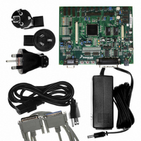
Manufacturer Part Number
MC56F8367EVME
Description
EVAL BOARD FOR MC56F83X
Manufacturer
Freescale Semiconductor
Type
DSPr
Specifications of MC56F8367EVME
Contents
Module and Misc Hardware
Processor To Be Evaluated
MC56F8145-67 and MC56F8345-67
Data Bus Width
16 bit
Interface Type
RS-232
Silicon Manufacturer
Freescale
Core Architecture
56800/E
Core Sub-architecture
56800/E
Silicon Core Number
MC56F
Silicon Family Name
MC56F83xx
Rohs Compliant
Yes
For Use With/related Products
MC56F83x5, MC56F83x6, MC56F83x7
Lead Free Status / RoHS Status
Lead free / RoHS Compliant


32
Table 2-2 Signal and Package Information for the 160-Pin LQFP and MBGA (Continued)
PHASEA1
PHASEB1
(GPIOC0)
(GPIOC1)
(SCLK1)
(MOSI1)
Signal
Name
(TB0)
(TB1)
No.
Pin
6
7
Ball No.
C1
D1
Schmitt
Schmitt
Schmitt
Schmitt
Schmitt
Schmitt
Schmitt
Schmitt
Output
Output
Output
Output
Output
Output
Input/
Input/
Input/
Input/
Input/
Input/
Type
Input
Input
56F8367 Technical Data, Rev. 8
enabled
enabled
During
pull-up
pull-up
Reset
State
Input,
Input,
Phase A1 — Quadrature Decoder 1, PHASEA input for decoder
1.
TB0 — Timer B, Channel 0
SPI 1 Serial Clock — In the master mode, this pin serves as an
output, clocking slaved listeners. In slave mode, this pin serves as
the data clock input. To activate the SPI function, set the
PHSA_ALT bit in the SIM_GPS register. For details, see
6.5.8.
Port C GPIO — This GPIO pin can be individually programmed
as an input or output pin.
In the 56F8367, the default state after reset is PHASEA1.
In the 56F8167, the default state is not one of the functions
offered and must be reconfigured.
To deactivate the internal pull-up resistor, clear bit 0 in the
GPIOC_PUR register.
Phase B1 — Quadrature Decoder 1, PHASEB input for decoder
1.
TB1 — Timer B, Channel 1
SPI 1 Master Out/Slave In — This serial data pin is an output
from a master device and an input to a slave device. The master
device places data on the MOSI line a half-cycle before the clock
edge the slave device uses to latch the data. To activate the SPI
function, set the PHSB_ALT bit in the SIM_GPS register. For
details, see
Port C GPIO — This GPIO pin can be individually programmed
as an input or output pin.
In the 56F8367, the default state after reset is PHASEB1.
In the 56F8167, the default state is not one of the functions
offered and must be reconfigured.
To deactivate the internal pull-up resistor, clear bit 1 in the
GPIOC_PUR register.
Part
6.5.8.
Signal Description
Freescale Semiconductor
Preliminary
Part
Related parts for MC56F8367EVME
Image
Part Number
Description
Manufacturer
Datasheet
Request
R

Part Number:
Description:
56f8300 16-bit Digital Signal Controllers
Manufacturer:
Freescale Semiconductor, Inc
Datasheet:
Part Number:
Description:
Manufacturer:
Freescale Semiconductor, Inc
Datasheet:
Part Number:
Description:
Manufacturer:
Freescale Semiconductor, Inc
Datasheet:
Part Number:
Description:
Manufacturer:
Freescale Semiconductor, Inc
Datasheet:
Part Number:
Description:
Manufacturer:
Freescale Semiconductor, Inc
Datasheet:
Part Number:
Description:
Manufacturer:
Freescale Semiconductor, Inc
Datasheet:
Part Number:
Description:
Manufacturer:
Freescale Semiconductor, Inc
Datasheet:
Part Number:
Description:
Manufacturer:
Freescale Semiconductor, Inc
Datasheet:
Part Number:
Description:
Manufacturer:
Freescale Semiconductor, Inc
Datasheet:
Part Number:
Description:
Manufacturer:
Freescale Semiconductor, Inc
Datasheet:
Part Number:
Description:
Manufacturer:
Freescale Semiconductor, Inc
Datasheet:
Part Number:
Description:
Manufacturer:
Freescale Semiconductor, Inc
Datasheet:
Part Number:
Description:
Manufacturer:
Freescale Semiconductor, Inc
Datasheet:
Part Number:
Description:
Manufacturer:
Freescale Semiconductor, Inc
Datasheet:
Part Number:
Description:
Manufacturer:
Freescale Semiconductor, Inc
Datasheet: