MC56F8367EVME Freescale Semiconductor, MC56F8367EVME Datasheet - Page 47
MC56F8367EVME
Manufacturer Part Number
MC56F8367EVME
Description
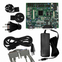
EVAL BOARD FOR MC56F83X
Manufacturer
Freescale Semiconductor
Type
DSPr
Specifications of MC56F8367EVME
Contents
Module and Misc Hardware
Processor To Be Evaluated
MC56F8145-67 and MC56F8345-67
Data Bus Width
16 bit
Interface Type
RS-232
Silicon Manufacturer
Freescale
Core Architecture
56800/E
Core Sub-architecture
56800/E
Silicon Core Number
MC56F
Silicon Family Name
MC56F83xx
Rohs Compliant
Yes
For Use With/related Products
MC56F83x5, MC56F83x6, MC56F83x7
Lead Free Status / RoHS Status
Lead free / RoHS Compliant


4.4 Data Map
Note: Data Flash is NOT available on the 56F8167 device.
4.5 Flash Memory Map
Figure 4-1
The Flash Memory is divided into three functional blocks. The Program and boot memories reside on the
Program Memory buses. They are controlled by one set of banked registers. Data Memory Flash resides
on the Data Memory buses and is controlled separately by its own set of banked registers.
The top nine words of the Program Memory Flash are treated as special memory locations. The content of
these words is used to control the operation of the Flash Controller. Because these words are part of the
Flash Memory content, their state is maintained during power down and reset. During chip initialization,
the content of these memory locations is loaded into Flash Memory control registers, detailed in the Flash
Memory chapter of the 56F8300 Peripheral User Manual. These configuration parameters are located
between $03_FFF7 and $03_FFFF.
Freescale Semiconductor
Preliminary
1. All addresses are 16-bit Word addresses, not byte addresses.
2. In the Operating Mode Register (OMR).
3. The Data RAM is organized as an 8K x 32-bit memory to allow single-cycle, long-word operations.
X:$FF FFFF
X:$FF FF00
X:$FF FEFF
X:$01 0000
X:$00 FFFF
X:$00 F000
X:$00 EFFF
X:$00 8000
X:$00 7FFF
X:$00 4000
X:$00 3FFF
X:$00 0000
Begin/End
Address
illustrates the Flash Memory (FM) map on the system bus.
EOnCE
256 locations allocated
External Memory
On-Chip Peripherals
4096 locations allocated
External Memory
On-Chip Data Flash
32KB
On-Chip Data RAM
32KB
3
Table 4-6 Data Memory Map
EX = 0
56F8367 Technical Data, Rev. 8
2
EOnCE
256 locations allocated
External Memory
On-Chip Peripherals
4096 locations allocated
External Memory
1
EX = 1
Data Map
47
Related parts for MC56F8367EVME
Image
Part Number
Description
Manufacturer
Datasheet
Request
R

Part Number:
Description:
56f8300 16-bit Digital Signal Controllers
Manufacturer:
Freescale Semiconductor, Inc
Datasheet:
Part Number:
Description:
Manufacturer:
Freescale Semiconductor, Inc
Datasheet:
Part Number:
Description:
Manufacturer:
Freescale Semiconductor, Inc
Datasheet:
Part Number:
Description:
Manufacturer:
Freescale Semiconductor, Inc
Datasheet:
Part Number:
Description:
Manufacturer:
Freescale Semiconductor, Inc
Datasheet:
Part Number:
Description:
Manufacturer:
Freescale Semiconductor, Inc
Datasheet:
Part Number:
Description:
Manufacturer:
Freescale Semiconductor, Inc
Datasheet:
Part Number:
Description:
Manufacturer:
Freescale Semiconductor, Inc
Datasheet:
Part Number:
Description:
Manufacturer:
Freescale Semiconductor, Inc
Datasheet:
Part Number:
Description:
Manufacturer:
Freescale Semiconductor, Inc
Datasheet:
Part Number:
Description:
Manufacturer:
Freescale Semiconductor, Inc
Datasheet:
Part Number:
Description:
Manufacturer:
Freescale Semiconductor, Inc
Datasheet:
Part Number:
Description:
Manufacturer:
Freescale Semiconductor, Inc
Datasheet:
Part Number:
Description:
Manufacturer:
Freescale Semiconductor, Inc
Datasheet:
Part Number:
Description:
Manufacturer:
Freescale Semiconductor, Inc
Datasheet: