EVAL-ADUC7032QSPZ Analog Devices Inc, EVAL-ADUC7032QSPZ Datasheet - Page 22
EVAL-ADUC7032QSPZ
Manufacturer Part Number
EVAL-ADUC7032QSPZ
Description
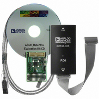
EVAL DEV QUICK START ADUC7032
Manufacturer
Analog Devices Inc
Series
QuickStart™ PLUS Kitr
Type
MCUr
Datasheet
1.EVAL-ADUC7032QSPZ.pdf
(116 pages)
Specifications of EVAL-ADUC7032QSPZ
Contents
Evaluation Board, Power Supply, Cable, Software, Emulator and Documentation
For Use With/related Products
ADuC7032
Lead Free Status / RoHS Status
Lead free / RoHS Compliant


ADuC7032-8L
Remap
The ARM exception vectors are all situated at the bottom of the
memory array, from Address 0x00000000 to Address 0x00000020.
By default, after a reset, the Flash/EE memory is logically mapped
to Address 0x00000000.
It is possible to logically remap the SRAM to Address 0x00000000
by setting Bit 0 of the SYSMAP0 MMR, which is located at
0xFFFF0220. To revert Flash/EE to Address 0x00000000, Bit 0 of
SYSMAP0 is cleared.
It may be desirable to remap RAM to Address 0x00000000 to
optimize the interrupt latency of the ADuC7032-8L, as code
can be run in full 32-bit ARM mode and at the maximum core
speed. It should be noted that when an exception occurs, the
core defaults to ARM mode.
Remap Operation
When a reset occurs on the ADuC7032-8L, execution starts
automatically in the factory-programmed internal configuration
code. This so-called kernel is hidden and cannot be accessed
by user code.
SYSMAP0 Register
Name: SYSMAP0
Address: 0xFFFF0220
Default Value: Updated by the kernel
Access: Read/write
Function: This 8-bit register allows user code to remap either RAM or Flash/EE space into the bottom of the ARM memory space,
starting at Address 0x00000000.
Table 11. SYSMAP0 MMR Bit Designations
Bit
7 to 1
0
Description
Reserved. These bits are reserved and should be written as 0 by user code.
Remap Bit.
Set by the user to remap the SRAM to 0x00000000.
Cleared automatically after reset to remap the Flash/EE memory to 0x00000000.
Rev.0 | Page 22 of 116
If the ADuC7032-8L is in normal mode, it executes the power-
on configuration routine of the kernel and then jumps to the
reset vector, Address 0x00000000, to execute the user reset
exception routine.
Because the Flash/EE is mirrored at the bottom of the memory
array at reset, the reset routine must always be written in Flash/EE.
Precautions must be taken to execute the remap command from
the absolute Flash/EE address, and not from the mirrored,
remapped segment of memory, because this segment may be
replaced by the SRAM. If a remap operation is executed while
operating code from the mirrored location, prefetch/data aborts
may occur; or the user may observe abnormal program operation.
This operation is reversible. The Flash/EE can be remapped to
Address 0x00000000 by clearing Bit 0 of the SYSMAP0 MMR.
Precautions must again be taken to execute the remap function
from outside the mirrored area.
Any kind of reset logically remaps the Flash/EE memory to the
bottom of the memory array.
Related parts for EVAL-ADUC7032QSPZ
Image
Part Number
Description
Manufacturer
Datasheet
Request
R

Part Number:
Description:
IC, ADJ LDO REG, 1.5V TO 5V 250mA MSOP-8
Manufacturer:
Vishay
Datasheet:

Part Number:
Description:
IC, ADJ LDO REG, 1.5V TO 5V 0.6A 8-TSSOP
Manufacturer:
Vishay
Datasheet:
Part Number:
Description:
IC, ADJ LDO REG, 1.5V TO 5V 250mA MSOP-8
Manufacturer:
Vishay
Datasheet:

Part Number:
Description:
IC ADJ LDO REG 1.5V TO 5V 150mA 5-SOT-23
Manufacturer:
Vishay
Datasheet:

Part Number:
Description:
BOARD EVAL AS1324-AD
Manufacturer:
austriamicrosystems
Datasheet:
Part Number:
Description:
IC, ADJ LDO REG, 1.5V TO 5V 0.6A 8-TSSOP
Manufacturer:
Vishay
Datasheet:

Part Number:
Description:
IC, ADJ LDO REG, 1.5V TO 5V, 0.3A, MSOP8
Manufacturer:
Vishay
Datasheet:
Part Number:
Description:
IC, ADJ LDO REG, 1.5V TO 5V, 0.3A, MSOP8
Manufacturer:
Vishay
Datasheet:
Part Number:
Description:
IC, ADJ LDO REG 1.215V TO 5V 0.3A MSOP-8
Manufacturer:
Vishay
Datasheet:
Part Number:
Description:
IC, ADJ LDO REG 1.215V TO 5V 0.3A MSOP-8
Manufacturer:
Vishay
Datasheet:

Part Number:
Description:
±1.7g Dual-Axis IMEMS Accelerometer Evaluation Board
Manufacturer:
Analog Devices Inc
Datasheet:

Part Number:
Description:
IC MULTIPLIER ANALOG 8-SOIC T/R
Manufacturer:
Analog Devices Inc
Datasheet:

Part Number:
Description:
IC ANALOG MULTIPLIER 8-DIP
Manufacturer:
Analog Devices Inc
Datasheet:
Part Number:
Description:
IC ANALOG MULTIPLIER 8-SOIC
Manufacturer:
Analog Devices Inc
Datasheet:
Part Number:
Description:
IC ANALOG MULTIPLIER 8-DIP
Manufacturer:
Analog Devices Inc
Datasheet: