EVAL-ADUC7032QSPZ Analog Devices Inc, EVAL-ADUC7032QSPZ Datasheet - Page 82
EVAL-ADUC7032QSPZ
Manufacturer Part Number
EVAL-ADUC7032QSPZ
Description
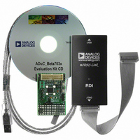
EVAL DEV QUICK START ADUC7032
Manufacturer
Analog Devices Inc
Series
QuickStart™ PLUS Kitr
Type
MCUr
Datasheet
1.EVAL-ADUC7032QSPZ.pdf
(116 pages)
Specifications of EVAL-ADUC7032QSPZ
Contents
Evaluation Board, Power Supply, Cable, Software, Emulator and Documentation
For Use With/related Products
ADuC7032
Lead Free Status / RoHS Status
Lead free / RoHS Compliant


ADuC7032-8L
GPIO Port1 Data Register
Name: GP1DAT
Address: 0xFFFF0D30
Default Value: 0x000000XX
Access: Read/write
Function: This 32-bit MMR configures the direction of the GPIO pins assigned to Port1 (see Table 58). This register also sets the output
value for GPIO pins configured as outputs and reads the status of GPIO pins configured as inputs.
Table 63. GP1DAT MMR Bit Designations
Bit
31 to 26
25
24
23 to 18
17
16
15 to 2
1
0
GPIO Port2 Data Register
Name: GP2DAT
Address: 0xFFFF0D40
Default Value: 0x000000XX
Access: Read/write
Function: This 32-bit MMR configures the direction of the GPIO pins assigned to Port2 (see Table 58). This register also sets the output
value for GPIO pins configured as outputs and reads the status of GPIO pins configured as inputs.
Table 64. GP2DAT MMR Bit Designations
Bit
31
30
29
28
27 to 26
25
24
23
Description
Reserved. This bit is reserved and should be written as 0 by user code.
Port2.6 Direction Select Bit.
Port2.5 Direction Select Bit.
Port2.4 Direction Select Bit.
Reserved. These bits are reserved and should be written as 0 by user code.
Port2.1 Direction Select Bit.
Port2.0 Direction Select Bit.
Reserved. This bit is reserved and should be written as 0 by user code.
Description
Reserved. These bits are reserved and should be written as 0 by user code.
Port1.1 Direction Select Bit.
Port1.0 Direction Select Bit.
Reserved. These bits are reserved and should be written as 0 by user code.
Port1.1 Data Output. The value written to this bit appears directly on the GPIO pin assigned to P1.1.
Port1.0 Data Output. The value written to this bit appears directly on the GPIO pin assigned to P1.0.
Reserved. These bits are reserved and should be written as 0 by user code.
Port1.1 Data Input. This bit is a read-only bit that reflects the current status of the GPIO pin assigned to P1.1. User code should
write 0 to this bit.
Port1.0 Data Input. This bit is a read-only bit that reflects the current status of the GPIO pin assigned to P1.0. User code should
write 0 to this bit.
Cleared to 0 by user code to configure the GPIO pin assigned to P1.1 as an input.
Set to 1 by user code to configure the GPIO pin assigned to P1.1 as an output.
Cleared to 0 by user code to configure the GPIO pin assigned to P1.0 as an input.
Set to 1 by user code to configure the GPIO pin assigned to P1.0 as an output.
Cleared to 0 by user code to configure the GPIO pin assigned to P2.6 as an input.
Set to 1 by user code to configure the GPIO pin assigned to P2.6 as an output.
Cleared to 0 by user code to configure the GPIO pin assigned to P2.5 as an input.
Set to 1 by user code to configure the GPIO pin assigned to P2.5 as an output. This configuration is used to support diagnostic
write capability to the high voltage I/O pins.
Cleared to 0 by user code to configure the GPIO pin assigned to P2.4 as an input. This configuration is used to support
diagnostic readback capability from the high voltage I/O pins (see HVCFG1[2:0]).
Set to 1 by user code to configure the GPIO pin assigned to P2.4 as an output.
Cleared to 0 by user code to configure the GPIO pin assigned to P2.1 as an input.
Set to 1 by user code to configure the GPIO pin assigned to P2.1 as an output.
Cleared to 0 by user code to configure the GPIO pin assigned to P2.0 as an input.
Set to 1 by user code to configure the GPIO pin assigned to P2.0 as an output.
Rev.0 | Page 82 of 116
Related parts for EVAL-ADUC7032QSPZ
Image
Part Number
Description
Manufacturer
Datasheet
Request
R

Part Number:
Description:
IC, ADJ LDO REG, 1.5V TO 5V 250mA MSOP-8
Manufacturer:
Vishay
Datasheet:

Part Number:
Description:
IC, ADJ LDO REG, 1.5V TO 5V 0.6A 8-TSSOP
Manufacturer:
Vishay
Datasheet:
Part Number:
Description:
IC, ADJ LDO REG, 1.5V TO 5V 250mA MSOP-8
Manufacturer:
Vishay
Datasheet:

Part Number:
Description:
IC ADJ LDO REG 1.5V TO 5V 150mA 5-SOT-23
Manufacturer:
Vishay
Datasheet:

Part Number:
Description:
BOARD EVAL AS1324-AD
Manufacturer:
austriamicrosystems
Datasheet:
Part Number:
Description:
IC, ADJ LDO REG, 1.5V TO 5V 0.6A 8-TSSOP
Manufacturer:
Vishay
Datasheet:

Part Number:
Description:
IC, ADJ LDO REG, 1.5V TO 5V, 0.3A, MSOP8
Manufacturer:
Vishay
Datasheet:
Part Number:
Description:
IC, ADJ LDO REG, 1.5V TO 5V, 0.3A, MSOP8
Manufacturer:
Vishay
Datasheet:
Part Number:
Description:
IC, ADJ LDO REG 1.215V TO 5V 0.3A MSOP-8
Manufacturer:
Vishay
Datasheet:
Part Number:
Description:
IC, ADJ LDO REG 1.215V TO 5V 0.3A MSOP-8
Manufacturer:
Vishay
Datasheet:

Part Number:
Description:
±1.7g Dual-Axis IMEMS Accelerometer Evaluation Board
Manufacturer:
Analog Devices Inc
Datasheet:

Part Number:
Description:
IC MULTIPLIER ANALOG 8-SOIC T/R
Manufacturer:
Analog Devices Inc
Datasheet:

Part Number:
Description:
IC ANALOG MULTIPLIER 8-DIP
Manufacturer:
Analog Devices Inc
Datasheet:
Part Number:
Description:
IC ANALOG MULTIPLIER 8-SOIC
Manufacturer:
Analog Devices Inc
Datasheet:
Part Number:
Description:
IC ANALOG MULTIPLIER 8-DIP
Manufacturer:
Analog Devices Inc
Datasheet: