EVAL-ADUC7032QSPZ Analog Devices Inc, EVAL-ADUC7032QSPZ Datasheet - Page 80
EVAL-ADUC7032QSPZ
Manufacturer Part Number
EVAL-ADUC7032QSPZ
Description
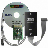
EVAL DEV QUICK START ADUC7032
Manufacturer
Analog Devices Inc
Series
QuickStart™ PLUS Kitr
Type
MCUr
Datasheet
1.EVAL-ADUC7032QSPZ.pdf
(116 pages)
Specifications of EVAL-ADUC7032QSPZ
Contents
Evaluation Board, Power Supply, Cable, Software, Emulator and Documentation
For Use With/related Products
ADuC7032
Lead Free Status / RoHS Status
Lead free / RoHS Compliant


ADuC7032-8L
GPIO Port1 Control Register
Name: GP1CON
Address: 0xFFFF0D04
Default Value: 0x10000000
Access: Read/write
Function: This 32-bit MMR selects the pin function for each Port1 pin.
Table 60. GP1CON MMR Bit Designations
GPIO Port2 Control Register
Name: GP2CON
Address: 0xFFFF0D08
Default Value: 0x01000000
Access: Read/write
Function: This 32-bit MMR selects the pin function for each Port2 pin.
Table 61. GP2CON MMR Bit Designations
Bit
31 to 5
4
3 to 1
0
Bit
31 to 21
20
19 to 17
16
15 to 5
4
3 to 1
0
Description
Reserved. These bits are reserved and should be written as 0 by user code.
GPIO_6 Function Select Bit.
Reserved. These bits are reserved and should be written as 0 by user code.
GPIO_5 Function Select Bit.
Description
Reserved. These bits are reserved and should be written as 0 by user code.
GPIO_12 Function Select Bit.
Reserved. These bits are reserved and should be written as 0 by user code.
GPIO_11 Function Select Bit.
Reserved. These bits are reserved and should be written as 0 by user code.
GPIO_8 Function Select Bit.
Reserved. These bits are reserved and should be written as 0 by user code.
GPIO_7 Function Select Bit.
Cleared to 0 by user code to configure the GPIO_6 pin as a general-purpose I/O (GPIO) pin.
Set to 1 by user code to configure the GPIO_6 pin as TxD, transmit data for UART serial port.
Cleared to 0 by user code to configure the GPIO_5 pin as a general-purpose I/O (GPIO) pin.
Set to 1 by user code to configure the GPIO_5 pin as RxD, receive data for UART serial port.
Cleared to 0 by user code to route the LIN transmit data to an internal general-purpose I/O (GPIO_12) pad that can then be
written via the GP2DAT MMR.
Set to 1 by user code to route the UART TxD (transmit data) to the LIN data pin. This configuration is used in LIN mode.
Cleared to 0 by user code to internally disable the LIN input data path. In this configuration, GPIO_11 is used to support
diagnostic readback on all external high voltage I/O pins (see HVCFG1[2:0]).
Set to 1 by user code to route input data from the LIN interface to both the LIN hardware timing/synchronization logic and to
the UART RxD (receive data). This mode must be configured by user code when using LIN.
Cleared to 0 by user code to internally disable the LIN input data path. In this configuration, GPIO_11 is used to support
diagnostic readback on all external high voltage I/O pins (see HVCFG1[2:0]).
Set to 1 by user code to route input data from the LIN interface to both the LIN hardware timing/synchronization logic and
the UART RxD (receive data). This mode must be configured by user code when using LIN.
Cleared to 0 by user code to configure the GPIO_7 pin as a general-purpose I/O (GPIO) pin.
Set to 1 by user code to route data driven into the GPIO_7 pin through the on-chip LIN transceiver to be output at the LIN
pin. This mode can be used to drive the LIN transceiver interface as a standalone component without any interaction from
MCU or UART.
Rev.0 | Page 80 of 116
Related parts for EVAL-ADUC7032QSPZ
Image
Part Number
Description
Manufacturer
Datasheet
Request
R

Part Number:
Description:
IC, ADJ LDO REG, 1.5V TO 5V 250mA MSOP-8
Manufacturer:
Vishay
Datasheet:

Part Number:
Description:
IC, ADJ LDO REG, 1.5V TO 5V 0.6A 8-TSSOP
Manufacturer:
Vishay
Datasheet:
Part Number:
Description:
IC, ADJ LDO REG, 1.5V TO 5V 250mA MSOP-8
Manufacturer:
Vishay
Datasheet:

Part Number:
Description:
IC ADJ LDO REG 1.5V TO 5V 150mA 5-SOT-23
Manufacturer:
Vishay
Datasheet:

Part Number:
Description:
BOARD EVAL AS1324-AD
Manufacturer:
austriamicrosystems
Datasheet:
Part Number:
Description:
IC, ADJ LDO REG, 1.5V TO 5V 0.6A 8-TSSOP
Manufacturer:
Vishay
Datasheet:

Part Number:
Description:
IC, ADJ LDO REG, 1.5V TO 5V, 0.3A, MSOP8
Manufacturer:
Vishay
Datasheet:
Part Number:
Description:
IC, ADJ LDO REG, 1.5V TO 5V, 0.3A, MSOP8
Manufacturer:
Vishay
Datasheet:
Part Number:
Description:
IC, ADJ LDO REG 1.215V TO 5V 0.3A MSOP-8
Manufacturer:
Vishay
Datasheet:
Part Number:
Description:
IC, ADJ LDO REG 1.215V TO 5V 0.3A MSOP-8
Manufacturer:
Vishay
Datasheet:

Part Number:
Description:
±1.7g Dual-Axis IMEMS Accelerometer Evaluation Board
Manufacturer:
Analog Devices Inc
Datasheet:

Part Number:
Description:
IC MULTIPLIER ANALOG 8-SOIC T/R
Manufacturer:
Analog Devices Inc
Datasheet:

Part Number:
Description:
IC ANALOG MULTIPLIER 8-DIP
Manufacturer:
Analog Devices Inc
Datasheet:
Part Number:
Description:
IC ANALOG MULTIPLIER 8-SOIC
Manufacturer:
Analog Devices Inc
Datasheet:
Part Number:
Description:
IC ANALOG MULTIPLIER 8-DIP
Manufacturer:
Analog Devices Inc
Datasheet: