EVAL-ADUC7032QSPZ Analog Devices Inc, EVAL-ADUC7032QSPZ Datasheet - Page 53
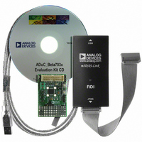
EVAL-ADUC7032QSPZ
Manufacturer Part Number
EVAL-ADUC7032QSPZ
Description
EVAL DEV QUICK START ADUC7032
Manufacturer
Analog Devices Inc
Series
QuickStart™ PLUS Kitr
Type
MCUr
Datasheet
1.EVAL-ADUC7032QSPZ.pdf
(116 pages)
Specifications of EVAL-ADUC7032QSPZ
Contents
Evaluation Board, Power Supply, Cable, Software, Emulator and Documentation
For Use With/related Products
ADuC7032
Lead Free Status / RoHS Status
Lead free / RoHS Compliant


Current Channel ADC Threshold Count Register
Name: ADC0THV
Address: 0xFFFF0558
Default Value: 0x00
Access: Read only
Function: This 8-bit MMR is incremented every time the
absolute value of an I-ADC conversion result |I| ≥ ADC0TH.
This register is decremented or reset to 0 every time the absolute
value of an I-ADC conversion result |I| < ADC0TH. The configu-
ration of this function is enabled via the current channel ADC
comparator bits in the ADCCFG MMR.
Current Channel ADC Accumulator Register
Name: ADC0ACC
Address: 0xFFFF055C
Default Value: 0x00000000
Access: Read only
Function: This 32-bit MMR holds the current channel accumu-
lator value. The I-ADC ready bit in the ADCSTA MMR should
be used to determine when it is safe to read this MMR. The
MMR value is reset to 0 by disabling the accumulator in the
ADCCFG MMR or reconfiguring the current channel ADC.
Current Channel ADC Accumulator Threshold Register
Name: ADC0ATH
Address: 0xFFFF0560
Default Value: 0x00000000
Access: Read/write
Function: This 32-bit MMR sets the threshold against which
the accumulated value of the I-ADC results is compared. In
unipolar mode, ADC0ATH [15:0] are compared and in twos
complement mode, ADC0ATH[14:0] are compared.
Low Power Voltage Reference Scaling Factor Register
Name: ADCREF
Address: 0xFFFF057C
Default Value: Part-specific, factory programmed
Access: Read/write
Function: This MMR allows user code to correct for the initial
error of the LPM reference. Value 0x8000 corresponds to no
error when compared to the normal mode reference. If the LPM
voltage reference is 1% below 1.200 V, the value of ADCREF is
approximately 0x7EB9. If the LPM voltage reference is 1% above
1.200 V, the value of ADCREF is approximately 0x8147.
This register corrects the effective value of the LPM reference at
the temperature at which the reference is measured during the
Analog Devices, Inc., production flow, which is 35°C. There is
no change to the temperature coefficient of the LPM reference
when using the ADCREF MMR.
This register should not be used if the precision reference is
being used in low power mode (if ADCMDE[5] is set).
Rev.0 | Page 53 of 116
ADC POWER MODES OF OPERATION
The ADCs can be configured into various reduced or full power
modes of operation by configuring ADCMDE[4:3] as appropriate.
The ARM7 MCU can itself also be configured in low power modes
of operation (POWCON[5:3]). The core power modes are inde-
pendently controlled and are not related to the ADC power modes
described in this section. The ADC power modes of operation are
described in more detail in the following paragraphs.
Every I-ADC result can also be compared to a preset threshold
level (ADC0TH), as configured via ADCCFG[4:3]. An MCU
interrupt is generated if the absolute (sign-independent) value
of the ADC result is greater than the preprogrammed comparator
threshold level. An extended function of this comparator
function allows user code to configure a threshold counter
(ADC0THV) that monitors the number of I-ADC results that
have occurred above or below the preset threshold level. Again,
an ADC interrupt is generated once the threshold counter
reaches a preset value (ADC0TCL).
Finally, a 32-bit accumulator (ADC0ACC) function can be
configured (ADCCFG[6:5]) allowing the I-ADC to add (or
subtract) multiple I-ADC sample results. User code can read
the accumulated value directly (via ADC0ACC) without any
further software processing.
ADC Startup Procedure
Before beginning the conversion process, the following
procedure should be followed:
1.
2.
3.
4.
5.
ADC Normal Power Mode
In normal mode, the current and voltage/temperature channels
are fully enabled. The ADC modulator clock is 512 kHz and
enables the ADCs to provide regular conversion results at a rate
of between 4 Hz and 8 kHz (see Table 40 for the ADCFLT MMR
bit designations). Both channels are under full control of the
MCU and can be reconfigured at any time. The default ADC
update rate for all channels in this mode is 1.0 kHz.
Configure the I-ADC to low power mode (ADC0CON =
0x8007; ADCMDE = 0x09).
Delay for 200 μs.
Switch the I-ADC into idle mode
(ADCMDE = 0x03), leaving ADC0CON unchanged.
If the voltage or temperature channels are to be used,
they should be enabled at this time.
Delay for 1 ms.
Switch ADCMDE to the desired mode, for example,
ADCMDE = 0x1.
ADuC7032-8L
Related parts for EVAL-ADUC7032QSPZ
Image
Part Number
Description
Manufacturer
Datasheet
Request
R

Part Number:
Description:
IC, ADJ LDO REG, 1.5V TO 5V 250mA MSOP-8
Manufacturer:
Vishay
Datasheet:

Part Number:
Description:
IC, ADJ LDO REG, 1.5V TO 5V 0.6A 8-TSSOP
Manufacturer:
Vishay
Datasheet:
Part Number:
Description:
IC, ADJ LDO REG, 1.5V TO 5V 250mA MSOP-8
Manufacturer:
Vishay
Datasheet:

Part Number:
Description:
IC ADJ LDO REG 1.5V TO 5V 150mA 5-SOT-23
Manufacturer:
Vishay
Datasheet:

Part Number:
Description:
BOARD EVAL AS1324-AD
Manufacturer:
austriamicrosystems
Datasheet:
Part Number:
Description:
IC, ADJ LDO REG, 1.5V TO 5V 0.6A 8-TSSOP
Manufacturer:
Vishay
Datasheet:

Part Number:
Description:
IC, ADJ LDO REG, 1.5V TO 5V, 0.3A, MSOP8
Manufacturer:
Vishay
Datasheet:
Part Number:
Description:
IC, ADJ LDO REG, 1.5V TO 5V, 0.3A, MSOP8
Manufacturer:
Vishay
Datasheet:
Part Number:
Description:
IC, ADJ LDO REG 1.215V TO 5V 0.3A MSOP-8
Manufacturer:
Vishay
Datasheet:
Part Number:
Description:
IC, ADJ LDO REG 1.215V TO 5V 0.3A MSOP-8
Manufacturer:
Vishay
Datasheet:

Part Number:
Description:
±1.7g Dual-Axis IMEMS Accelerometer Evaluation Board
Manufacturer:
Analog Devices Inc
Datasheet:

Part Number:
Description:
IC MULTIPLIER ANALOG 8-SOIC T/R
Manufacturer:
Analog Devices Inc
Datasheet:

Part Number:
Description:
IC ANALOG MULTIPLIER 8-DIP
Manufacturer:
Analog Devices Inc
Datasheet:
Part Number:
Description:
IC ANALOG MULTIPLIER 8-SOIC
Manufacturer:
Analog Devices Inc
Datasheet:
Part Number:
Description:
IC ANALOG MULTIPLIER 8-DIP
Manufacturer:
Analog Devices Inc
Datasheet: