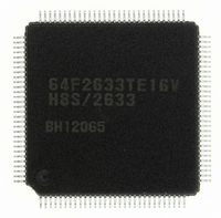
R5F61668RN50FPV Renesas Electronics America, R5F61668RN50FPV Datasheet - Page 1159

R5F61668RN50FPV
Manufacturer Part Number
R5F61668RN50FPV
Description
IC H8SX/1668 MCU FLASH 144LQFP
Manufacturer
Renesas Electronics America
Series
H8® H8SX/1600r
Datasheet
1.R5F61668RN50FPV.pdf
(1506 pages)
Specifications of R5F61668RN50FPV
Core Processor
H8SX
Core Size
16/32-Bit
Speed
50MHz
Connectivity
EBI/EMI, I²C, IrDA, SCI, SmartCard, USB
Peripherals
DMA, LVD, POR, PWM, WDT
Number Of I /o
92
Program Memory Size
1MB (1M x 8)
Program Memory Type
FLASH
Ram Size
56K x 8
Voltage - Supply (vcc/vdd)
3 V ~ 3.6 V
Data Converters
A/D 8x10b; D/A 2x8b
Oscillator Type
External
Operating Temperature
-20°C ~ 75°C
Package / Case
144-LQFP
For Use With
R0K561668S000BE - KIT STARTER FOR H8SX/1668R0K561664S001BE - KIT STARTER FOR H8SX/1651HS0005KCU11H - EMULATOR E10A-USB H8S(X),SH2(A)
Lead Free Status / RoHS Status
Lead free / RoHS Compliant
Eeprom Size
-
Available stocks
Company
Part Number
Manufacturer
Quantity
Price
Company:
Part Number:
R5F61668RN50FPV
Manufacturer:
Renesas Electronics America
Quantity:
10 000
- Current page: 1159 of 1506
- Download datasheet (9Mb)
25.7.2
The programming/erasing interface parameters specify the operating frequency, storage place for
program data, start address of programming destination, and erase block number, and exchanges
the execution result. These parameters use the general registers of the CPU (ER0 and ER1) or the
on-chip RAM area. The initial values of programming/erasing interface parameters are undefined
at a reset or a transition to software standby mode.
Since registers of the CPU except for ER0 and ER1 are saved in the stack area during download of
an on-chip program, initialization, programming, or erasing, allocate the stack area before
performing these operations (the maximum stack size is 128 bytes). The return value of the
processing result is written in R0. The programming/erasing interface parameters are used in
download control, initialization before programming or erasing, programming, and erasing. Table
25.4 shows the usable parameters and target modes. The meaning of the bits in the flash pass and
fail result parameter (FPFR) varies in initialization, programming, and erasure.
Table 25.4 Parameters and Target Modes
Note:
(a)
The on-chip program is automatically downloaded by setting the SCO bit in FCCS to 1. The on-
chip RAM area to download the on-chip program is the 4-Kbyte area starting from the start
address specified by FTDAR. Download is set by the programming/erasing interface registers, and
the download pass and fail result parameter (DPFR) indicates the return value.
Parameter
DPFR
FPFR
FPEFEQ
FMPAR
FMPDR
FEBS
Download Control
*
Programming/Erasing Interface Parameters
A single byte of the start address of the on-chip RAM specified by FTDAR
Download
O
O
Initialization
O
O
O
O
O
Programming
Erasure
O
O
Rev. 2.00 Sep. 24, 2008 Page 1125 of 1468
R/W
R/W
R/W
R/W
R/W
R/W
R/W
Initial
Value
Undefined
Undefined
Undefined
Undefined
Undefined
Undefined
Section 25 Flash Memory
REJ09B0412-0200
Allocation
On-chip RAM*
R0L of CPU
ER0 of CPU
ER1 of CPU
ER0 of CPU
ER0 of CPU
Related parts for R5F61668RN50FPV
Image
Part Number
Description
Manufacturer
Datasheet
Request
R

Part Number:
Description:
KIT STARTER FOR M16C/29
Manufacturer:
Renesas Electronics America
Datasheet:

Part Number:
Description:
KIT STARTER FOR R8C/2D
Manufacturer:
Renesas Electronics America
Datasheet:

Part Number:
Description:
R0K33062P STARTER KIT
Manufacturer:
Renesas Electronics America
Datasheet:

Part Number:
Description:
KIT STARTER FOR R8C/23 E8A
Manufacturer:
Renesas Electronics America
Datasheet:

Part Number:
Description:
KIT STARTER FOR R8C/25
Manufacturer:
Renesas Electronics America
Datasheet:

Part Number:
Description:
KIT STARTER H8S2456 SHARPE DSPLY
Manufacturer:
Renesas Electronics America
Datasheet:

Part Number:
Description:
KIT STARTER FOR R8C38C
Manufacturer:
Renesas Electronics America
Datasheet:

Part Number:
Description:
KIT STARTER FOR R8C35C
Manufacturer:
Renesas Electronics America
Datasheet:

Part Number:
Description:
KIT STARTER FOR R8CL3AC+LCD APPS
Manufacturer:
Renesas Electronics America
Datasheet:

Part Number:
Description:
KIT STARTER FOR RX610
Manufacturer:
Renesas Electronics America
Datasheet:

Part Number:
Description:
KIT STARTER FOR R32C/118
Manufacturer:
Renesas Electronics America
Datasheet:

Part Number:
Description:
KIT DEV RSK-R8C/26-29
Manufacturer:
Renesas Electronics America
Datasheet:

Part Number:
Description:
KIT STARTER FOR SH7124
Manufacturer:
Renesas Electronics America
Datasheet:

Part Number:
Description:
KIT STARTER FOR H8SX/1622
Manufacturer:
Renesas Electronics America
Datasheet:

Part Number:
Description:
KIT DEV FOR SH7203
Manufacturer:
Renesas Electronics America
Datasheet:


