R5F61668RN50FPV Renesas Electronics America, R5F61668RN50FPV Datasheet - Page 20
R5F61668RN50FPV
Manufacturer Part Number
R5F61668RN50FPV
Description
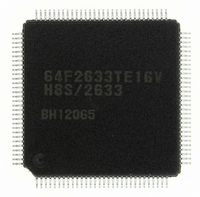
IC H8SX/1668 MCU FLASH 144LQFP
Manufacturer
Renesas Electronics America
Series
H8® H8SX/1600r
Datasheet
1.R5F61668RN50FPV.pdf
(1506 pages)
Specifications of R5F61668RN50FPV
Core Processor
H8SX
Core Size
16/32-Bit
Speed
50MHz
Connectivity
EBI/EMI, I²C, IrDA, SCI, SmartCard, USB
Peripherals
DMA, LVD, POR, PWM, WDT
Number Of I /o
92
Program Memory Size
1MB (1M x 8)
Program Memory Type
FLASH
Ram Size
56K x 8
Voltage - Supply (vcc/vdd)
3 V ~ 3.6 V
Data Converters
A/D 8x10b; D/A 2x8b
Oscillator Type
External
Operating Temperature
-20°C ~ 75°C
Package / Case
144-LQFP
For Use With
R0K561668S000BE - KIT STARTER FOR H8SX/1668R0K561664S001BE - KIT STARTER FOR H8SX/1651HS0005KCU11H - EMULATOR E10A-USB H8S(X),SH2(A)
Lead Free Status / RoHS Status
Lead free / RoHS Compliant
Eeprom Size
-
Available stocks
Company
Part Number
Manufacturer
Quantity
Price
Company:

Part Number:
R5F61668RN50FPV
Manufacturer:
Renesas Electronics America
Quantity:
10 000


Section 12 Data Transfer Controller (DTC)...................................................... 559
12.1
12.2
12.3
12.4
12.5
12.6
12.7
12.8
12.9
Rev. 2.00 Sep. 24, 2008 Page xviii of xxxii
Features............................................................................................................................. 559
Register Descriptions........................................................................................................ 561
12.2.1
12.2.2
12.2.3
12.2.4
12.2.5
12.2.6
12.2.7
12.2.8
12.2.9
Activation Sources............................................................................................................ 569
Location of Transfer Information and DTC Vector Table................................................ 569
Operation .......................................................................................................................... 574
12.5.1
12.5.2
12.5.3
12.5.4
12.5.5
12.5.6
12.5.7
12.5.8
12.5.9
12.5.10 DTC Bus Release Timing ................................................................................. 587
12.5.11 DTC Priority Level Control to the CPU ........................................................... 587
DTC Activation by Interrupt............................................................................................. 588
Examples of Use of the DTC............................................................................................ 589
12.7.1
12.7.2
12.7.3
Interrupt Sources............................................................................................................... 592
Usage Notes ...................................................................................................................... 592
12.9.1
12.9.2
12.9.3
12.9.4
12.9.5
12.9.6
DTC Mode Register A (MRA) ......................................................................... 562
DTC Mode Register B (MRB).......................................................................... 563
DTC Source Address Register (SAR)............................................................... 564
DTC Destination Address Register (DAR)....................................................... 565
DTC Transfer Count Register A (CRA) ........................................................... 565
DTC Transfer Count Register B (CRB)............................................................ 566
DTC enable registers A to F (DTCERA to DTCERF) ..................................... 566
DTC Control Register (DTCCR) ...................................................................... 567
DTC Vector Base Register (DTCVBR)............................................................ 569
Bus Cycle Division ........................................................................................... 576
Transfer Information Read Skip Function ........................................................ 578
Transfer Information Writeback Skip Function................................................ 579
Normal Transfer Mode ..................................................................................... 579
Repeat Transfer Mode ...................................................................................... 580
Block Transfer Mode ........................................................................................ 582
Chain Transfer .................................................................................................. 583
Operation Timing.............................................................................................. 584
Number of DTC Execution Cycles ................................................................... 586
Normal Transfer Mode ..................................................................................... 589
Chain Transfer .................................................................................................. 589
Chain Transfer when Counter = 0..................................................................... 590
Module Stop State Setting ................................................................................ 592
On-Chip RAM .................................................................................................. 592
DMAC Transfer End Interrupt.......................................................................... 592
DTCE Bit Setting.............................................................................................. 592
Chain Transfer .................................................................................................. 593
Transfer Information Start Address, Source Address, and Destination
Address ............................................................................................................. 593
Related parts for R5F61668RN50FPV
Image
Part Number
Description
Manufacturer
Datasheet
Request
R

Part Number:
Description:
KIT STARTER FOR M16C/29
Manufacturer:
Renesas Electronics America
Datasheet:

Part Number:
Description:
KIT STARTER FOR R8C/2D
Manufacturer:
Renesas Electronics America
Datasheet:

Part Number:
Description:
R0K33062P STARTER KIT
Manufacturer:
Renesas Electronics America
Datasheet:

Part Number:
Description:
KIT STARTER FOR R8C/23 E8A
Manufacturer:
Renesas Electronics America
Datasheet:

Part Number:
Description:
KIT STARTER FOR R8C/25
Manufacturer:
Renesas Electronics America
Datasheet:

Part Number:
Description:
KIT STARTER H8S2456 SHARPE DSPLY
Manufacturer:
Renesas Electronics America
Datasheet:

Part Number:
Description:
KIT STARTER FOR R8C38C
Manufacturer:
Renesas Electronics America
Datasheet:

Part Number:
Description:
KIT STARTER FOR R8C35C
Manufacturer:
Renesas Electronics America
Datasheet:

Part Number:
Description:
KIT STARTER FOR R8CL3AC+LCD APPS
Manufacturer:
Renesas Electronics America
Datasheet:
Part Number:
Description:
KIT STARTER FOR RX610
Manufacturer:
Renesas Electronics America
Datasheet:

Part Number:
Description:
KIT STARTER FOR R32C/118
Manufacturer:
Renesas Electronics America
Datasheet:

Part Number:
Description:
KIT DEV RSK-R8C/26-29
Manufacturer:
Renesas Electronics America
Datasheet:

Part Number:
Description:
KIT STARTER FOR SH7124
Manufacturer:
Renesas Electronics America
Datasheet:

Part Number:
Description:
KIT STARTER FOR H8SX/1622
Manufacturer:
Renesas Electronics America
Datasheet:

Part Number:
Description:
KIT DEV FOR SH7203
Manufacturer:
Renesas Electronics America
Datasheet: