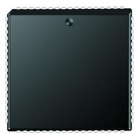
PIC18F6680-I/L Microchip Technology, PIC18F6680-I/L Datasheet - Page 177

PIC18F6680-I/L
Manufacturer Part Number
PIC18F6680-I/L
Description
Microcontrollers (MCU) 64KB 3328 RAM 52 I/O
Manufacturer
Microchip Technology
Datasheet
1.PCM18XK1.pdf
(496 pages)
Specifications of PIC18F6680-I/L
Processor Series
PIC18F
Core
PIC
Data Bus Width
8 bit
Data Ram Size
3.25 KB
Interface Type
I2C/SPI/AUSART/CAN
Maximum Clock Frequency
40 MHz
Number Of Programmable I/os
53
Number Of Timers
5
Operating Supply Voltage
4.2 V to 5.5 V
Maximum Operating Temperature
+ 85 C
Mounting Style
SMD/SMT
3rd Party Development Tools
52715-96, 52716-328, 52717-734, 52712-325, EWPIC18
Development Tools By Supplier
PG164130, DV164035, DV244005, DV164005, PG164120, ICE2000, ICE4000, DV164136
Minimum Operating Temperature
- 40 C
On-chip Adc
12-ch x 10-bit
Program Memory Type
Flash
Program Memory Size
64 KB
Package / Case
PLCC-68
Lead Free Status / RoHS Status
Lead free / RoHS Compliant
Available stocks
Company
Part Number
Manufacturer
Quantity
Price
Company:
Part Number:
PIC18F6680-I/L
Manufacturer:
RUBYCON
Quantity:
46 000
Part Number:
PIC18F6680-I/L
Manufacturer:
MICROCH
Quantity:
20 000
- Current page: 177 of 496
- Download datasheet (9Mb)
16.0
The CCP1 module is implemented as a standard CCP
module with enhanced PWM capabilities. These capa-
bilities allow for 2 or 4 output channels, user selectable
polarity, dead-band control, and automatic shutdown
and restart and are discussed in detail in Section 16.2
“Enhanced PWM Mode”.
REGISTER 16-1:
2004 Microchip Technology Inc.
ENHANCED CAPTURE/
COMPARE/PWM (ECCP)
MODULE
bit 7-6
bit 5-4
bit 3-0
CCP1CON REGISTER
Legend:
R = Readable bit
- n = Value at POR
bit 7
P1M1:P1M0: Enhanced PWM Output Configuration bits
If CCP1M<3:2> = 00, 01, 10:
xx = P1A assigned as capture/compare input; P1B, P1C, P1D assigned as port pins
If CCP1M<3:2> = 11:
00 = Single output; P1A modulated, P1B, P1C, P1D assigned as port pins
01 = Full-bridge output forward; P1D modulated; P1A active; P1B, P1C inactive
10 = Half-bridge output; P1A, P1B modulated with dead-band control; P1C, P1D assigned as
11 = Full-bridge output reverse; P1B modulated; P1C active; P1A, P1D inactive
DC1B1:DC1B0: PWM Duty Cycle bit 1 and bit 0
Capture mode:
Unused.
Compare mode:
Unused.
PWM mode:
These bits are the two LSbs of the 10-bit PWM duty cycle. The eight MSbs of the duty cycle are
found in CCPR1L.
CCP1M3:CCP1M0: Enhanced CCP Mode Select bits
0000 = Capture/Compare/PWM off (resets CCP1 module)
0001 = Reserved
0010 = Compare mode, toggle output on match
0011 = Capture mode, CAN message time-stamp
0100 = Capture mode, every falling edge
0101 = Capture mode, every rising edge
0110 = Capture mode, every 4th rising edge
0111 = Capture mode, every 16th rising edge
1000 = Compare mode, initialize CCP pin low, on compare match, force CCP pin high
1001 = Compare mode, initialize CCP pin high, on compare match, force CCP pin low
1010 = Compare mode, generate software interrupt only, CCP pin is unaffected
1011 = Compare mode, trigger special event, resets TMR1 or TMR3
1100 = PWM mode; P1A, P1C active-high; P1B, P1D active-high
1101 = PWM mode; P1A, P1C active-high; P1B, P1D active-low
1110 = PWM mode; P1A, P1C active-low; P1B, P1D active-high
1111 = PWM mode; P1A, P1C active-low; P1B, P1D active-low
R/W-0
P1M1
port pins
R/W-0
P1M0
PIC18F6585/8585/6680/8680
DC1B1
R/W-0
W = Writable bit
‘1’ = Bit is set
DC1B0
R/W-0
The control register for CCP1 is shown in Register 16-1.
In addition to the expanded functions of the
CCP1CON register, the CCP1 module has two
• ECCP1DEL
• ECCP1AS
additional registers associated with enhanced PWM
operation and auto-shutdown features:
CCP1M3
U = Unimplemented bit, read as ‘0’
‘0’ = Bit is cleared
R/W-0
CCP1M2
R/W-0
x = Bit is unknown
CCP1M1
R/W-0
DS30491C-page 175
CCP1M0
R/W-0
bit 0
Related parts for PIC18F6680-I/L
Image
Part Number
Description
Manufacturer
Datasheet
Request
R

Part Number:
Description:
20-Pin USB Flash Microcontrollers
Manufacturer:
MICROCHIP [Microchip Technology]
Datasheet:

Part Number:
Description:
PIC18F With 128-segment LCD Driver And 12-bit ADC, 8KB Flash, 768B RAM, CCP, MSS
Manufacturer:
Microchip Technology
Datasheet:

Part Number:
Description:
PIC18F With 128-segment LCD Driver And 12-bit ADC, 16KB Flash, 768B RAM, CCP, MS
Manufacturer:
Microchip Technology
Datasheet:

Part Number:
Description:
PIC18F With 192-segment LCD Driver And 12-bit ADC, 8KB Flash, 768B RAM, CCP, MSS
Manufacturer:
Microchip Technology
Datasheet:

Part Number:
Description:
PIC18F With 192-segment LCD Driver And 12-bit ADC, 16KB Flash, 768B RAM, CCP, MS
Manufacturer:
Microchip Technology
Datasheet:

Part Number:
Description:
Microcontrollers (MCU) 48KB 3328 RAM 52 I/O
Manufacturer:
Microchip Technology
Datasheet:

Part Number:
Description:
32kB Flash, 2kB RAM, 1kB EE, NanoWatt XLP, LCD 64 QFN 9x9x0.9mm T/R
Manufacturer:
Microchip Technology
Datasheet:

Part Number:
Description:
32kB Flash, 2kB RAM, 1kB EE, NanoWatt XLP, LCD 64 TQFP 10x10x1mm T/R
Manufacturer:
Microchip Technology
Datasheet:

Part Number:
Description:
128kB Flash, 4kB RAM, 1kB EE, 16MIPS, NanoWatt XLP, LCD, 5V 80 TQFP 12x12x1mm T/
Manufacturer:
Microchip Technology
Datasheet:

Part Number:
Description:
32kB Flash, 2kB RAM, 1kB EE, NanoWatt XLP, LCD 64 QFN 9x9x0.9mm TUBE
Manufacturer:
Microchip Technology
Datasheet:

Part Number:
Description:
32kB Flash, 2kB RAM, 1kB EE, NanoWatt XLP, LCD 64 TQFP 10x10x1mm TRAY
Manufacturer:
Microchip Technology

Part Number:
Description:
128kB Flash, 4kB RAM, 1kB EE, 16MIPS, NanoWatt XLP, LCD, 5V 80 TQFP 12x12x1mm TR
Manufacturer:
Microchip Technology

Part Number:
Description:
Manufacturer:
Microchip Technology Inc.
Datasheet:


