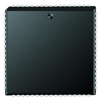
PIC18F6680-I/L Microchip Technology, PIC18F6680-I/L Datasheet - Page 385

PIC18F6680-I/L
Manufacturer Part Number
PIC18F6680-I/L
Description
Microcontrollers (MCU) 64KB 3328 RAM 52 I/O
Manufacturer
Microchip Technology
Datasheet
1.PCM18XK1.pdf
(496 pages)
Specifications of PIC18F6680-I/L
Processor Series
PIC18F
Core
PIC
Data Bus Width
8 bit
Data Ram Size
3.25 KB
Interface Type
I2C/SPI/AUSART/CAN
Maximum Clock Frequency
40 MHz
Number Of Programmable I/os
53
Number Of Timers
5
Operating Supply Voltage
4.2 V to 5.5 V
Maximum Operating Temperature
+ 85 C
Mounting Style
SMD/SMT
3rd Party Development Tools
52715-96, 52716-328, 52717-734, 52712-325, EWPIC18
Development Tools By Supplier
PG164130, DV164035, DV244005, DV164005, PG164120, ICE2000, ICE4000, DV164136
Minimum Operating Temperature
- 40 C
On-chip Adc
12-ch x 10-bit
Program Memory Type
Flash
Program Memory Size
64 KB
Package / Case
PLCC-68
Lead Free Status / RoHS Status
Lead free / RoHS Compliant
Available stocks
Company
Part Number
Manufacturer
Quantity
Price
Company:
Part Number:
PIC18F6680-I/L
Manufacturer:
RUBYCON
Quantity:
46 000
Part Number:
PIC18F6680-I/L
Manufacturer:
MICROCH
Quantity:
20 000
- Current page: 385 of 496
- Download datasheet (9Mb)
CPFSGT
Syntax:
Operands:
Operation:
Status Affected:
Encoding:
Description:
Words:
Cycles:
Example:
2004 Microchip Technology Inc.
Q Cycle Activity:
If skip:
If skip and followed by 2-word instruction:
Before Instruction
After Instruction
operation
operation
operation
Decode
PC
W
If REG
If REG
No
No
No
Q1
Q1
Q1
PC
PC
=
=
=
=
register ‘f’
operation
operation
operation
Compare f with W, skip if f > W
[ label ] CPFSGT
0
a
(f)
skip if (f) > (W)
(unsigned comparison)
None
Compares the contents of data
memory location ‘f’ to the contents
of the W by performing an
unsigned subtraction.
If the contents of ‘f’ are greater than
the contents of WREG
fetched instruction is discarded and
a NOP is executed instead, making
this a two-cycle instruction. If ‘a’ is
‘0’, the Access Bank will be
selected, overriding the BSR value.
If ‘a’ = 1, then the bank will be
selected as per the BSR value
(default).
1
1(2)
Note: 3 cycles if skip and followed
HERE
NGREATER
GREATER
Read
0110
No
No
No
Q2
Q2
Q2
Address (HERE)
?
W;
Address (GREATER)
W;
Address (NGREATER)
f
[0,1]
W),
255
by a 2-word instruction.
010a
operation
operation
operation
CPFSGT REG, 0
:
:
Process
Data
No
No
No
Q3
Q3
Q3
ffff
f [,a]
,
then the
operation
operation
operation
operation
PIC18F6585/8585/6680/8680
No
No
No
No
Q4
Q4
Q4
ffff
CPFSLT
Syntax:
Operands:
Operation:
Status Affected:
Encoding:
Description:
Words:
Cycles:
Example:
Q Cycle Activity:
If skip:
If skip and followed by 2-word instruction:
Before Instruction
After Instruction
operation
operation
operation
Decode
No
No
No
PC
W
If REG
If REG
Q1
Q1
Q1
PC
PC
=
=
<
=
=
register ‘f’
operation
operation
operation
Compare f with W, skip if f < W
[ label ] CPFSLT
0
a
(f) – W),
skip if (f) < (W)
(unsigned comparison)
None
Compares the contents of data
memory location ‘f’ to the contents
of W by performing an unsigned
subtraction.
If the contents of ‘f’ are less than
the contents of W, then the fetched
instruction is discarded and a NOP
is executed instead, making this a
two-cycle instruction. If ‘a’ is ‘0’, the
Access Bank will be selected. If ’a’
is ‘1’, the BSR will not be overrid-
den (default).
1
1(2)
Note: 3 cycles if skip and followed
HERE
NLESS
LESS
Read
0110
No
No
No
Q2
Q2
Q2
Address (HERE)
?
W;
Address (LESS)
W;
Address (NLESS)
f
[0,1]
255
by a 2-word instruction.
CPFSLT REG, 1
:
:
000a
operation
operation
operation
Process
Data
No
No
No
Q3
Q3
Q3
DS30491C-page 383
ffff
f [,a]
operation
operation
operation
operation
No
No
No
No
Q4
Q4
Q4
ffff
Related parts for PIC18F6680-I/L
Image
Part Number
Description
Manufacturer
Datasheet
Request
R

Part Number:
Description:
20-Pin USB Flash Microcontrollers
Manufacturer:
MICROCHIP [Microchip Technology]
Datasheet:

Part Number:
Description:
PIC18F With 128-segment LCD Driver And 12-bit ADC, 8KB Flash, 768B RAM, CCP, MSS
Manufacturer:
Microchip Technology
Datasheet:

Part Number:
Description:
PIC18F With 128-segment LCD Driver And 12-bit ADC, 16KB Flash, 768B RAM, CCP, MS
Manufacturer:
Microchip Technology
Datasheet:

Part Number:
Description:
PIC18F With 192-segment LCD Driver And 12-bit ADC, 8KB Flash, 768B RAM, CCP, MSS
Manufacturer:
Microchip Technology
Datasheet:

Part Number:
Description:
PIC18F With 192-segment LCD Driver And 12-bit ADC, 16KB Flash, 768B RAM, CCP, MS
Manufacturer:
Microchip Technology
Datasheet:

Part Number:
Description:
Microcontrollers (MCU) 48KB 3328 RAM 52 I/O
Manufacturer:
Microchip Technology
Datasheet:

Part Number:
Description:
32kB Flash, 2kB RAM, 1kB EE, NanoWatt XLP, LCD 64 QFN 9x9x0.9mm T/R
Manufacturer:
Microchip Technology
Datasheet:

Part Number:
Description:
32kB Flash, 2kB RAM, 1kB EE, NanoWatt XLP, LCD 64 TQFP 10x10x1mm T/R
Manufacturer:
Microchip Technology
Datasheet:

Part Number:
Description:
128kB Flash, 4kB RAM, 1kB EE, 16MIPS, NanoWatt XLP, LCD, 5V 80 TQFP 12x12x1mm T/
Manufacturer:
Microchip Technology
Datasheet:

Part Number:
Description:
32kB Flash, 2kB RAM, 1kB EE, NanoWatt XLP, LCD 64 QFN 9x9x0.9mm TUBE
Manufacturer:
Microchip Technology
Datasheet:

Part Number:
Description:
32kB Flash, 2kB RAM, 1kB EE, NanoWatt XLP, LCD 64 TQFP 10x10x1mm TRAY
Manufacturer:
Microchip Technology

Part Number:
Description:
128kB Flash, 4kB RAM, 1kB EE, 16MIPS, NanoWatt XLP, LCD, 5V 80 TQFP 12x12x1mm TR
Manufacturer:
Microchip Technology

Part Number:
Description:
Manufacturer:
Microchip Technology Inc.
Datasheet:


