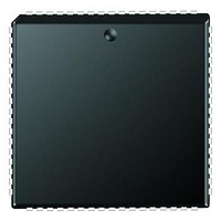
PIC18F6680-I/L Microchip Technology, PIC18F6680-I/L Datasheet - Page 253

PIC18F6680-I/L
Manufacturer Part Number
PIC18F6680-I/L
Description
Microcontrollers (MCU) 64KB 3328 RAM 52 I/O
Manufacturer
Microchip Technology
Datasheet
1.PCM18XK1.pdf
(496 pages)
Specifications of PIC18F6680-I/L
Processor Series
PIC18F
Core
PIC
Data Bus Width
8 bit
Data Ram Size
3.25 KB
Interface Type
I2C/SPI/AUSART/CAN
Maximum Clock Frequency
40 MHz
Number Of Programmable I/os
53
Number Of Timers
5
Operating Supply Voltage
4.2 V to 5.5 V
Maximum Operating Temperature
+ 85 C
Mounting Style
SMD/SMT
3rd Party Development Tools
52715-96, 52716-328, 52717-734, 52712-325, EWPIC18
Development Tools By Supplier
PG164130, DV164035, DV244005, DV164005, PG164120, ICE2000, ICE4000, DV164136
Minimum Operating Temperature
- 40 C
On-chip Adc
12-ch x 10-bit
Program Memory Type
Flash
Program Memory Size
64 KB
Package / Case
PLCC-68
Lead Free Status / RoHS Status
Lead free / RoHS Compliant
Available stocks
Company
Part Number
Manufacturer
Quantity
Price
Company:
Part Number:
PIC18F6680-I/L
Manufacturer:
RUBYCON
Quantity:
46 000
Part Number:
PIC18F6680-I/L
Manufacturer:
MICROCH
Quantity:
20 000
- Current page: 253 of 496
- Download datasheet (9Mb)
REGISTER 19-3:
2004 Microchip Technology Inc.
bit 7
bit 6
bit 5-3
bit 2-0
ADCON2 REGISTER
bit 7
ADFM: A/D Result Format Select bit
1 = Right justified
0 = Left justified
Unimplemented: Read as ‘0’
ACQT2:ACQT0: A/D Acquisition Time Select bits
000 = 0 T
001 = 2 T
010 = 4 T
011 = 6 T
100 = 8 T
101 = 12 T
110 = 16 T
111 = 20 T
ADCS2:ADCS0: A/D Conversion Clock Select bits
000 = F
001 = F
010 = F
011 = F
100 = F
101 = F
110 = F
111 = F
Legend:
R = Readable bit
- n = Value at POR
R/W-0
ADFM
Note 1: If the A/D F
OSC
OSC
OSC
RC
OSC
OSC
OSC
RC
AD
AD
AD
AD
AD
AD
AD
AD
(clock derived from A/D RC oscillator)
(clock derived from A/D RC oscillator)
added before the A/D clock starts. This allows the SLEEP instruction to be executed
before starting a conversion.
/2
/8
/32
/4
/16
/64
(1)
U-0
—
PIC18F6585/8585/6680/8680
RC
ACQT2
R/W-0
clock source is selected, a delay of one T
W = Writable bit
‘1’ = Bit is set
ACQT1
R/W-0
ACQT0
(1)
(1)
R/W-0
U = Unimplemented bit, read as ‘0’
‘0’ = Bit is cleared
ADCS2
R/W-0
CY
x = Bit is unknown
ADCS1
R/W-0
(instruction cycle) is
DS30491C-page 251
ADCS0
R/W-0
bit 0
Related parts for PIC18F6680-I/L
Image
Part Number
Description
Manufacturer
Datasheet
Request
R

Part Number:
Description:
20-Pin USB Flash Microcontrollers
Manufacturer:
MICROCHIP [Microchip Technology]
Datasheet:

Part Number:
Description:
PIC18F With 128-segment LCD Driver And 12-bit ADC, 8KB Flash, 768B RAM, CCP, MSS
Manufacturer:
Microchip Technology
Datasheet:

Part Number:
Description:
PIC18F With 128-segment LCD Driver And 12-bit ADC, 16KB Flash, 768B RAM, CCP, MS
Manufacturer:
Microchip Technology
Datasheet:

Part Number:
Description:
PIC18F With 192-segment LCD Driver And 12-bit ADC, 8KB Flash, 768B RAM, CCP, MSS
Manufacturer:
Microchip Technology
Datasheet:

Part Number:
Description:
PIC18F With 192-segment LCD Driver And 12-bit ADC, 16KB Flash, 768B RAM, CCP, MS
Manufacturer:
Microchip Technology
Datasheet:

Part Number:
Description:
Microcontrollers (MCU) 48KB 3328 RAM 52 I/O
Manufacturer:
Microchip Technology
Datasheet:

Part Number:
Description:
32kB Flash, 2kB RAM, 1kB EE, NanoWatt XLP, LCD 64 QFN 9x9x0.9mm T/R
Manufacturer:
Microchip Technology
Datasheet:

Part Number:
Description:
32kB Flash, 2kB RAM, 1kB EE, NanoWatt XLP, LCD 64 TQFP 10x10x1mm T/R
Manufacturer:
Microchip Technology
Datasheet:

Part Number:
Description:
128kB Flash, 4kB RAM, 1kB EE, 16MIPS, NanoWatt XLP, LCD, 5V 80 TQFP 12x12x1mm T/
Manufacturer:
Microchip Technology
Datasheet:

Part Number:
Description:
32kB Flash, 2kB RAM, 1kB EE, NanoWatt XLP, LCD 64 QFN 9x9x0.9mm TUBE
Manufacturer:
Microchip Technology
Datasheet:

Part Number:
Description:
32kB Flash, 2kB RAM, 1kB EE, NanoWatt XLP, LCD 64 TQFP 10x10x1mm TRAY
Manufacturer:
Microchip Technology

Part Number:
Description:
128kB Flash, 4kB RAM, 1kB EE, 16MIPS, NanoWatt XLP, LCD, 5V 80 TQFP 12x12x1mm TR
Manufacturer:
Microchip Technology

Part Number:
Description:
Manufacturer:
Microchip Technology Inc.
Datasheet:


