Z85C3008VSG Zilog, Z85C3008VSG Datasheet - Page 132
Z85C3008VSG
Manufacturer Part Number
Z85C3008VSG
Description
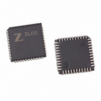
IC 8MHZ Z8500 CMOS SCC 44-PLCC
Manufacturer
Zilog
Series
SCCr
Specifications of Z85C3008VSG
Processor Type
Z80
Features
Error Detection and Multiprotocol Support
Speed
8MHz
Voltage
5V
Mounting Type
Surface Mount
Package / Case
44-LCC (J-Lead)
Maximum Operating Temperature
+ 70 C
Minimum Operating Temperature
0 C
Mounting Style
SMD/SMT
Cpu Speed
8MHz
Digital Ic Case Style
LCC
No. Of Pins
44
Supply Voltage Range
5V
Operating Temperature Range
0°C To +70°C
Svhc
No SVHC (18-Jun-2010)
Base Number
85
Rohs Compliant
Yes
Clock Frequency
8MHz
Lead Free Status / RoHS Status
Lead free / RoHS Compliant
Other names
269-3932
Z85C3008VSG
Z85C3008VSG
Available stocks
Company
Part Number
Manufacturer
Quantity
Price
Company:

Part Number:
Z85C3008VSG
Manufacturer:
Zilog
Quantity:
800
Company:
Part Number:
Z85C3008VSG
Manufacturer:
MAX
Quantity:
74


UM010901-0601
5.3.4 Read Register 3
RR3 is the interrupt Pending register. The status of each
of the interrupt Pending bits in the SCC is reported in this
register. This register exists only in Channel A. If this
register is accessed in Channel B, all 0s are returned. The
two unused bits are always returned as 0. Figure 5-22
shows the bit positions for RR3.
5.3.5 Read Register 4 (ESCC and 85C30 Only)
On the ESCC, Read Register 4 reflects the contents of
Write Register 4 provided the Extended Read option is en-
abled. Otherwise, this register returns an image of RR0.
On the NMOS/CMOS version, a read to this location re-
turns an image of RR0.
Read Register 3
D7 D6 D5 D4 D3 D2 D1 D0
Read Register 2
D7 D6 D5 D4
*
*
Always 0 In B Channel
Modified In B Channel
Figure 5-21. Read Register 2
Figure 5-22. Read Register 3
D3 D2 D1 D0
Channel B Ext/Status IP
Channel B Tx IP
Channel B Rx IP
Channel A Ext/Status IP
Channel A Tx IP
Channel A Rx IP
0
0
V0
V1
V2
V3
V4
V5
V6
V7
Interrupt
Vector
*
*
5.3.6 Read Register 5 (ESCC and 85C30 Only)
On the ESCC, Read Register 5 reflects the contents of
Write Register 5 provided the Extended Read option is en-
abled. Otherwise, this register returns an image of RR1.
On the NMOS/CMOS version, a read to this register re-
turns an image of RR1.
5.3.7 Read Register 6 (Not on NMOS)
On the CMOS and ESCC, Read Register 6 contains the
least significant byte of the frame byte count that is current-
ly at the top of the Status FIFO. RR6 is shown in Figure 5-
23. This register is readable only if the FIFO is enabled (re-
fer to the description Write Register 15, bit D2 and Section
4.4.3). Otherwise, this register is an image of RR2.
On the NMOS version, a read to this register location re-
turns an image of RR2.
5.3.8 Read Register 7 (Not on NMOS)
On the CMOS and ESCC, Read Register 7 contains the
most significant six bits of the frame byte count that is
currently at the top of the Status FIFO. Bit D7 is the FIFO
Overflow Status and bit D6 is the FIFO Data Available
Status. The status indications are given in Table 5-13. RR7
is shown in Figure 5-24. This register is readable only if the
FIFO is enabled (refer to the description Write Register 15,
bit D2). Otherwise this register is an image of RR3. Note,
for proper operation of the FIFO and byte count logic, the
registers should be read in the following order: RR7, RR6,
RR1.
Figure 5-23. Read Register 6 (Not on NMOS)
Read Register 6
D7 D6 D5
*
SDLC FIFO Status and Byte Count (LSB)
is enabled (WR15 bit D2 set to 1)
Can only be accessed if the SDLC FIFO enhancement
D4 D3 D2 D1
*
SCC™/ESCC™ User’s Manual
D0
Register Descriptions
BC0
BC1
BC2
BC3
BC4
BC5
BC6
BC7
5-25
5
Related parts for Z85C3008VSG
Image
Part Number
Description
Manufacturer
Datasheet
Request
R

Part Number:
Description:
Manufacturer:
Zilog, Inc.
Datasheet:

Part Number:
Description:
Cmos Scc Serial Communications Controller
Manufacturer:
ZiLOG Semiconductor
Datasheet:
Part Number:
Description:
Communication Controllers, ZILOG INTELLIGENT PERIPHERAL CONTROLLER (ZIP)
Manufacturer:
Zilog, Inc.
Datasheet:

Part Number:
Description:
KIT DEV FOR Z8 ENCORE 16K TO 64K
Manufacturer:
Zilog
Datasheet:

Part Number:
Description:
KIT DEV Z8 ENCORE XP 28-PIN
Manufacturer:
Zilog
Datasheet:

Part Number:
Description:
DEV KIT FOR Z8 ENCORE 8K/4K
Manufacturer:
Zilog
Datasheet:

Part Number:
Description:
KIT DEV Z8 ENCORE XP 28-PIN
Manufacturer:
Zilog
Datasheet:

Part Number:
Description:
DEV KIT FOR Z8 ENCORE 4K TO 8K
Manufacturer:
Zilog
Datasheet:
Part Number:
Description:
CMOS Z8 microcontroller. ROM 16 Kbytes, RAM 256 bytes, speed 16 MHz, 32 lines I/O, 3.0V to 5.5V
Manufacturer:
Zilog, Inc.
Datasheet:
Part Number:
Description:
Low-cost microcontroller. 512 bytes ROM, 61 bytes RAM, 8 MHz
Manufacturer:
Zilog, Inc.
Datasheet:
Part Number:
Description:
Z8 4K OTP Microcontroller
Manufacturer:
Zilog, Inc.
Datasheet:
Part Number:
Description:
CMOS SUPER8 ROMLESS MCU
Manufacturer:
Zilog, Inc.
Datasheet:
Part Number:
Description:
SL1866 CMOSZ8 OTP Microcontroller
Manufacturer:
Zilog, Inc.
Datasheet: