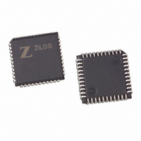
Z85C3008VSG Zilog, Z85C3008VSG Datasheet - Page 293

Z85C3008VSG
Manufacturer Part Number
Z85C3008VSG
Description
IC 8MHZ Z8500 CMOS SCC 44-PLCC
Manufacturer
Zilog
Series
SCCr
Specifications of Z85C3008VSG
Processor Type
Z80
Features
Error Detection and Multiprotocol Support
Speed
8MHz
Voltage
5V
Mounting Type
Surface Mount
Package / Case
44-LCC (J-Lead)
Maximum Operating Temperature
+ 70 C
Minimum Operating Temperature
0 C
Mounting Style
SMD/SMT
Cpu Speed
8MHz
Digital Ic Case Style
LCC
No. Of Pins
44
Supply Voltage Range
5V
Operating Temperature Range
0°C To +70°C
Svhc
No SVHC (18-Jun-2010)
Base Number
85
Rohs Compliant
Yes
Clock Frequency
8MHz
Lead Free Status / RoHS Status
Lead free / RoHS Compliant
Other names
269-3932
Z85C3008VSG
Z85C3008VSG
Available stocks
Company
Part Number
Manufacturer
Quantity
Price
Company:
Part Number:
Z85C3008VSG
Manufacturer:
Zilog
Quantity:
800
Company:
Part Number:
Z85C3008VSG
Manufacturer:
MAX
Quantity:
74
- Current page: 293 of 317
- Download datasheet (4Mb)
Application Note
On-Chip Oscillator Design
Output Level. The signal at the amplifier output should
swing from ground to V
gain in the amplifier. As the oscillator starts up, the signal
amplitude grows until clipping occurs, at which point, the
6-158
PRACTICE: CIRCUIT ELEMENT AND LAY OUT CONSIDERATIONS (Continued)
Must Be Avoided)
(Parallel Traces
Signal C
C L
C
L
CC
Signals A B
EXTAL
. This indicates there is adequate
XTAL
Clock Generator Circuit
2
3
2
3
Z80180
Figure 9. Circuit Board Design Rules
Z80180
64
64
loop gain is effectively reduced to unity and constant
oscillation is achieved. A signal of less than 2.5 Vp-p is an
indication that low gain may be a problem. Either C1/C2
should be made smaller or a low R crystal should be used.
To prevent induced noice, the crystal and load
capacitors should be physically located as
close to the LSI as possible.
Signal lines should not run parallel to the clock
oscillator inputs. In particullar, the clock input
circuitry and the system clock output (pin 64)
should be separated as much as possible.
V
clock oscillator input circuitry.
Resistivity between XTAL or EXTAL and the
other pin should be greater than 10 M
cc
power lines should be separated from the
Board Design Example
1
2
3
(Top View)
20 mm
Z80180
max
GND
64
Layout Should
Lighted Areas
Signal Line
Avoid High
20 mm max
CLK
UM010901-0601
Related parts for Z85C3008VSG
Image
Part Number
Description
Manufacturer
Datasheet
Request
R

Part Number:
Description:
Manufacturer:
Zilog, Inc.
Datasheet:

Part Number:
Description:
Cmos Scc Serial Communications Controller
Manufacturer:
ZiLOG Semiconductor
Datasheet:

Part Number:
Description:
Communication Controllers, ZILOG INTELLIGENT PERIPHERAL CONTROLLER (ZIP)
Manufacturer:
Zilog, Inc.
Datasheet:

Part Number:
Description:
KIT DEV FOR Z8 ENCORE 16K TO 64K
Manufacturer:
Zilog
Datasheet:

Part Number:
Description:
KIT DEV Z8 ENCORE XP 28-PIN
Manufacturer:
Zilog
Datasheet:

Part Number:
Description:
DEV KIT FOR Z8 ENCORE 8K/4K
Manufacturer:
Zilog
Datasheet:

Part Number:
Description:
KIT DEV Z8 ENCORE XP 28-PIN
Manufacturer:
Zilog
Datasheet:

Part Number:
Description:
DEV KIT FOR Z8 ENCORE 4K TO 8K
Manufacturer:
Zilog
Datasheet:

Part Number:
Description:
CMOS Z8 microcontroller. ROM 16 Kbytes, RAM 256 bytes, speed 16 MHz, 32 lines I/O, 3.0V to 5.5V
Manufacturer:
Zilog, Inc.
Datasheet:

Part Number:
Description:
Low-cost microcontroller. 512 bytes ROM, 61 bytes RAM, 8 MHz
Manufacturer:
Zilog, Inc.
Datasheet:

Part Number:
Description:
Z8 4K OTP Microcontroller
Manufacturer:
Zilog, Inc.
Datasheet:

Part Number:
Description:
CMOS SUPER8 ROMLESS MCU
Manufacturer:
Zilog, Inc.
Datasheet:

Part Number:
Description:
SL1866 CMOSZ8 OTP Microcontroller
Manufacturer:
Zilog, Inc.
Datasheet:


