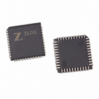
Z85C3008VSG Zilog, Z85C3008VSG Datasheet - Page 15

Z85C3008VSG
Manufacturer Part Number
Z85C3008VSG
Description
IC 8MHZ Z8500 CMOS SCC 44-PLCC
Manufacturer
Zilog
Series
SCCr
Specifications of Z85C3008VSG
Processor Type
Z80
Features
Error Detection and Multiprotocol Support
Speed
8MHz
Voltage
5V
Mounting Type
Surface Mount
Package / Case
44-LCC (J-Lead)
Maximum Operating Temperature
+ 70 C
Minimum Operating Temperature
0 C
Mounting Style
SMD/SMT
Cpu Speed
8MHz
Digital Ic Case Style
LCC
No. Of Pins
44
Supply Voltage Range
5V
Operating Temperature Range
0°C To +70°C
Svhc
No SVHC (18-Jun-2010)
Base Number
85
Rohs Compliant
Yes
Clock Frequency
8MHz
Lead Free Status / RoHS Status
Lead free / RoHS Compliant
Other names
269-3932
Z85C3008VSG
Z85C3008VSG
Available stocks
Company
Part Number
Manufacturer
Quantity
Price
Company:
Part Number:
Z85C3008VSG
Manufacturer:
Zilog
Quantity:
800
Company:
Part Number:
Z85C3008VSG
Manufacturer:
MAX
Quantity:
74
- Current page: 15 of 317
- Download datasheet (4Mb)
UM010901-0601
1.4 PIN DESCRIPTIONS
The SCC pins are divided into seven functional groups:
Address/Data, Bus Timing and Reset, Device Control, In-
terrupt, Serial Data (both channels), Peripheral Control
(both channels), and Clocks (both channels). Figures 1-2
and 1-3 show the pins in each functional group for both
Z80X30 and Z85X30. Notice the pin functions unique to
each bus interface version in the Address/Data group, Bus
Timing and Reset group, and Control groups.
The Address/Data group consists of the bidirectional lines
used to transfer data between the CPU and the SCC (Ad-
dresses in the Z80X30 are latched by /AS). The direction
of these lines depends on whether the operation is a Read
or Write.
Bus Timing
Data Bus
and Reset
Interrupt
Control
Figure 1-2. Z85X30 Pin Functions
D7
D6
D5
D4
D3
D2
D1
D0
/RD
/WR
A//B
/CE
D//C
/INT
/INTACK
IEI
IEO
Z85X30
/DTR//REQA
The timing and control groups designate the type of trans-
action to occur and when it will occur. The interrupt group
provides inputs and outputs to conform to the Z-Bus
specifications for handling and prioritizing interrupts. The
remaining groups are divided into channel A and channel
B groups for serial data (transmit or receive), peripheral
control (such as DMA or modem), and the input and output
lines for the receive and transmit clocks.
The signal functionality and pin assignments (Figures 1-4
to 1-7) stay constant within the same bus interface group
(i.e., Z80X30, Z85X30), except for some timing and/or DC
specification differences. For details, please reference the
individual product specifications.
/DTR//REQB
/W//REQA
/W//REQB
/TRxCA
/TRxCB
/RTxCA
/SYNCA
/RTxCB
/SYNCB
/DCDA
/DCDB
TxDA
/RTSA
/CTSA
TxDB
RxDB
/RTSB
/CTSB
RxDA
SCC™/ESCC™ User’s Manual
Serial
Data
Channel
Clocks
Channel
Controls
for Modem,
DMA and
Other
Serial
Data
Channel
Clocks
Channel
Controls
for Modem,
DMA and
Other
General Description
1-5
®
1
Related parts for Z85C3008VSG
Image
Part Number
Description
Manufacturer
Datasheet
Request
R

Part Number:
Description:
Manufacturer:
Zilog, Inc.
Datasheet:

Part Number:
Description:
Cmos Scc Serial Communications Controller
Manufacturer:
ZiLOG Semiconductor
Datasheet:

Part Number:
Description:
Communication Controllers, ZILOG INTELLIGENT PERIPHERAL CONTROLLER (ZIP)
Manufacturer:
Zilog, Inc.
Datasheet:

Part Number:
Description:
KIT DEV FOR Z8 ENCORE 16K TO 64K
Manufacturer:
Zilog
Datasheet:

Part Number:
Description:
KIT DEV Z8 ENCORE XP 28-PIN
Manufacturer:
Zilog
Datasheet:

Part Number:
Description:
DEV KIT FOR Z8 ENCORE 8K/4K
Manufacturer:
Zilog
Datasheet:

Part Number:
Description:
KIT DEV Z8 ENCORE XP 28-PIN
Manufacturer:
Zilog
Datasheet:

Part Number:
Description:
DEV KIT FOR Z8 ENCORE 4K TO 8K
Manufacturer:
Zilog
Datasheet:

Part Number:
Description:
CMOS Z8 microcontroller. ROM 16 Kbytes, RAM 256 bytes, speed 16 MHz, 32 lines I/O, 3.0V to 5.5V
Manufacturer:
Zilog, Inc.
Datasheet:

Part Number:
Description:
Low-cost microcontroller. 512 bytes ROM, 61 bytes RAM, 8 MHz
Manufacturer:
Zilog, Inc.
Datasheet:

Part Number:
Description:
Z8 4K OTP Microcontroller
Manufacturer:
Zilog, Inc.
Datasheet:

Part Number:
Description:
CMOS SUPER8 ROMLESS MCU
Manufacturer:
Zilog, Inc.
Datasheet:

Part Number:
Description:
SL1866 CMOSZ8 OTP Microcontroller
Manufacturer:
Zilog, Inc.
Datasheet:


