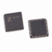
Z85C3008VSG Zilog, Z85C3008VSG Datasheet - Page 245

Z85C3008VSG
Manufacturer Part Number
Z85C3008VSG
Description
IC 8MHZ Z8500 CMOS SCC 44-PLCC
Manufacturer
Zilog
Series
SCCr
Specifications of Z85C3008VSG
Processor Type
Z80
Features
Error Detection and Multiprotocol Support
Speed
8MHz
Voltage
5V
Mounting Type
Surface Mount
Package / Case
44-LCC (J-Lead)
Maximum Operating Temperature
+ 70 C
Minimum Operating Temperature
0 C
Mounting Style
SMD/SMT
Cpu Speed
8MHz
Digital Ic Case Style
LCC
No. Of Pins
44
Supply Voltage Range
5V
Operating Temperature Range
0°C To +70°C
Svhc
No SVHC (18-Jun-2010)
Base Number
85
Rohs Compliant
Yes
Clock Frequency
8MHz
Lead Free Status / RoHS Status
Lead free / RoHS Compliant
Other names
269-3932
Z85C3008VSG
Z85C3008VSG
Available stocks
Company
Part Number
Manufacturer
Quantity
Price
Company:
Part Number:
Z85C3008VSG
Manufacturer:
Zilog
Quantity:
800
Company:
Part Number:
Z85C3008VSG
Manufacturer:
MAX
Quantity:
74
- Current page: 245 of 317
- Download datasheet (4Mb)
Application Note
Using SCC with Z8000 in SDLC Protocol
INITIALIZATION
The SCC can be initialized for use in different modes by
setting various bits in its write registers. First, a hardware
reset must be performed by setting bits 7 and 6 of WR9 to
one; the rest of the bits are disabled by writing a logic zero.
SDLC protocol is established by selecting a SDLC mode,
sync mode enable, and a x1 clock in WR4. A data rate of
9600 baud, NRZ encoding, and a character length of eight
bits are among the other options that are selected in this
example (Table 2).
Note that WR9 is accessed twice, first to perform a
hardware reset and again at the end of the initialization
sequence to enable the interrupts. The programming
sequence depicted in Table 2 establishes the necessary
parameters for the receiver and transmitter so that they are
ready to perform communication tasks when enabled.
Register
WR9
WR4
WR10
WR6
WR7
WR2
WR11
WR12
WR13
WR14
WR15
WR5
WR3
WR1
WR9
6-110
Table 2. Programming Sequence for Initialization
Value
(Hex)
C0
20
80
AB
7E
20
16
CE
0
03
00
60
C1
08
09
Effect
Hardware reset
x1 clock, SDLC mode,
sync mode enable
NRZ, CRC preset to one
Any station address e.g. “AB”
SDLC flag (01111110) = “7E”
Interrupt vector “20”
Tx clock from BRG output, /TRxC pin
= BRG out
Lower byte of time constant = “CE” for
9600 baud
Upper byte = 0
BRG source bit =1 for PCKL as input,
BRG enable
External Interrupt Disable
Transmit 8 bits/character SDLC CRC
Rx 8 bits/character, Rx enable
(Automatic Hunt mode)
ext int. disable
MIE, VIS, status Low
The Z8002 CPU must be operated in System mode to
execute privileged I/O instructions. So the Flag and
Control Word (FCW) should be loaded with system normal
(S//N), and the Vectored Interrupt Enable (VIE) bits set.
The Program Status Area Pointer (PSAP) is loaded with
address %4400 using the Load Control Instruction
(LDCTL). If the Z8000 Development Module is intended to
be used, the PSAP need not be loaded by the programmer
because the development module’s monitor loads it
automatically after the NMI button is pressed.
Since VIS and Status Low are selected in WR9, the
vectors listed in Table 3 will be returned during the
Interrupt Acknowledge cycle. Of the four interrupts listed,
only two, Ch A Receive Character Available and Ch A
Special Receive Condition, are used in the example given
here.
Vector
(Hex)
28
2A
2C
2E
* Assuming that PSAP has been set to 4400 hex, “PS
Address” refers to the location in the Program Status Area
where the service routine address is stored for that
particular interrupt.
PS
Address
446E
4472
4476
447A
Table 3. Interrupt Vectors
Interrupt
Ch A Transmit Buffer Empty
Ch A External Status Change
Ch A Receive Char. Available
Ch A Special Receive Condition
UM010901-0601
Related parts for Z85C3008VSG
Image
Part Number
Description
Manufacturer
Datasheet
Request
R

Part Number:
Description:
Manufacturer:
Zilog, Inc.
Datasheet:

Part Number:
Description:
Cmos Scc Serial Communications Controller
Manufacturer:
ZiLOG Semiconductor
Datasheet:

Part Number:
Description:
Communication Controllers, ZILOG INTELLIGENT PERIPHERAL CONTROLLER (ZIP)
Manufacturer:
Zilog, Inc.
Datasheet:

Part Number:
Description:
KIT DEV FOR Z8 ENCORE 16K TO 64K
Manufacturer:
Zilog
Datasheet:

Part Number:
Description:
KIT DEV Z8 ENCORE XP 28-PIN
Manufacturer:
Zilog
Datasheet:

Part Number:
Description:
DEV KIT FOR Z8 ENCORE 8K/4K
Manufacturer:
Zilog
Datasheet:

Part Number:
Description:
KIT DEV Z8 ENCORE XP 28-PIN
Manufacturer:
Zilog
Datasheet:

Part Number:
Description:
DEV KIT FOR Z8 ENCORE 4K TO 8K
Manufacturer:
Zilog
Datasheet:

Part Number:
Description:
CMOS Z8 microcontroller. ROM 16 Kbytes, RAM 256 bytes, speed 16 MHz, 32 lines I/O, 3.0V to 5.5V
Manufacturer:
Zilog, Inc.
Datasheet:

Part Number:
Description:
Low-cost microcontroller. 512 bytes ROM, 61 bytes RAM, 8 MHz
Manufacturer:
Zilog, Inc.
Datasheet:

Part Number:
Description:
Z8 4K OTP Microcontroller
Manufacturer:
Zilog, Inc.
Datasheet:

Part Number:
Description:
CMOS SUPER8 ROMLESS MCU
Manufacturer:
Zilog, Inc.
Datasheet:

Part Number:
Description:
SL1866 CMOSZ8 OTP Microcontroller
Manufacturer:
Zilog, Inc.
Datasheet:


