PEB3081FV14XP Lantiq, PEB3081FV14XP Datasheet
PEB3081FV14XP
Specifications of PEB3081FV14XP


Related parts for PEB3081FV14XP

PEB3081FV14XP Summary of contents
Page 1
...
Page 2
Edition 2000-09-27 Published by Infineon Technologies AG, St.-Martin-Strasse 53, D-81541 München, Germany © Infineon Technologies AG 9/28/00. All Rights Reserved. Attention please! The information herein is given to describe certain components and shall not be considered as warranted characteristics. Terms ...
Page 3
...
Page 4
PEB 3081 Preliminary Revision History: Previous Version: Page Subjects (major changes since last revision) For questions on technology, delivery and prices please contact the Infineon Technologies Offices in Germany or the Infineon Technologies Companies and Representatives worldwide: see our webpage ...
Page 5
Table of Contents 1 Overview . . . . . . . . . . . . . . . . . . . . . . . . . . . . . . . . . . . ...
Page 6
Table of Contents 3.5.3 State Machine NT Mode . . . . . . . . . . . . . . . . . . . . . . . . . . . . . . . . ...
Page 7
Table of Contents 4.1.11 SQRR1 - S/Q-Channel Receive Register 141 4.1.12 SQXR1- S/Q-Channel TX Register ...
Page 8
Table of Contents 4.4.5 MODE1 - Mode1 Register 4.4.6 MODE2 - Mode2 Register 4.4 Identification Register 4.4.8 SRES - Software Reset Register . . . . . . . . . . . . . . . . ...
Page 9
List of Figures Figure 1 Logic Symbol of the SBCX ...
Page 10
List of Figures Figure 39 Example of Activation/Deactivation initiated by the Network Termination (NT). Activation/Deactivation completely under Software Control . . . . . . . . 81 Figure 40 IOM -2 Frame Structure in Terminal Mode . . . ...
Page 11
List of Tables Table 1 Comparison of the SBCX-X with the previous version SBCX Table 2 SBCX-X Pin Definitions and Functions . . . . . . . . . . . ...
Page 12
Preliminary 1 Overview The S/T Bus Interface Circuit Extended (SBCX-X) implements the four-wire S/T interface used to link voice/data ISDN terminals, network terminators and PBX trunk lines to a central office the successor of the SBCX PEB 2081 ...
Page 13
Preliminary Table 1 Comparison of the SBCX-X with the previous version SBCX: (cont’d) Controller data access to IOM-2 timeslots Data control and manipulation Auxiliary Interface IOM channel select (LT modes) LED pin Output pin for D-channel active indication Control input ...
Page 14
Preliminary Table 1 Comparison of the SBCX-X with the previous version SBCX: (cont’d) Layer 1 state machine Layer 1 state machine in software Reset Signals Reset Sources Interrupt Output Signals Data Sheet SBCX-X PEB 3081 With changes for correspondence with ...
Page 15
Preliminary S/T Bus Interface Circuit Extended SBCX-X Version 1.3 1.1 Features • Full duplex S/T interface transceiver according to ITU-T I.430 • Successor of SBCX PEB 2081 in 3.3V technology • Conversion of the frame structure between ...
Page 16
Preliminary • Power supply 3.3 V • 3.3 V output drivers, inputs are 5 V safe • Advanced CMOS technology Data Sheet 16 PEB 3081 PEF 3081 Overview 2000-09-27 ...
Page 17
Preliminary 1.2 Logic Symbol The logic symbol gives an overview of the SBCX-X functions. It must be noted that not all functions are available simultaneously, but depend on the selected mode. Pins which are marked with a “ * “ ...
Page 18
Preliminary 1.3 Typical Applications The SBCX-X is designed for the user area of the ISDN basic access. By programming the corresponding operating mode it may be used at both ends of these interfaces. Figure 2 illustrates the general application fields ...
Page 19
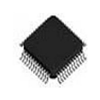
Preliminary 2 Pin Configuration BCL / SCLK DU DD FSC DCL VSS VSS VDD MODE0 MODE1 / EAW ACL Figure 3 Pin Configuration of the SBCX-X (P-MQFP-44) Data Sheet P-MQFP- ...
Page 20
Preliminary BCL / SCLK DU DD FSC DCL VSS VSS VDD MODE0 MODE1 / EAW ACL n.c. Figure 4 Pin Configuration of the SBCX-X (P-TQFP-48) Data Sheet P-TQFP- ...
Page 21
Preliminary Table 2 SBCX-X Pin Definitions and Functions Pin No. Symbol MQFP- TQFP Host Interface 9 10 SCL 10 11 SDR 11 12 SDX INT 5 5 RES IOM-2 Interface 37 40 FSC ...
Page 22
Preliminary Table 2 SBCX-X Pin Definitions and Functions (cont’d) Pin No. Symbol MQFP- TQFP BCL/ SCLK SDS1 18 20 SDS2 Miscellaneous 28 31 SX1 29 32 SX2 32 ...
Page 23
Preliminary Table 2 SBCX-X Pin Definitions and Functions (cont’d) Pin No. Symbol MQFP- TQFP AUX0 21 23 AUX1 22 24 AUX2 42 45 MODE0 43 46 MODE1 EAW 6 6 RSTO 17 19 C768 14 16 ...
Page 24
Preliminary Table 2 SBCX-X Pin Definitions and Functions (cont’d) Pin No. Symbol MQFP- TQFP DCI 16 18 SGO 44 47 ACL 15, n.c. 30, 48 Power Supply V 8, 13, ...
Page 25
Preliminary 3 Description of Functional Blocks 3.1 General Functions and Device Architecture Figure 5 shows the architecture of the SBCX-X containing the following functions: • S/T-interface transceiver supporting TE, LT-T, LT-S, NT and intelligent NT modes • Serial Control Interface ...
Page 26
Preliminary General Auxiliary Purpose Interface I/Os Figure 5 Functional Block Diagram of the SBCX-X Data Sheet Description of Functional Blocks Peripheral Devices IOM-2 Interface IOM-2 Handler MONITOR TIC C/I Handler Serial Host Interface Reset (SCI) Interrupt generation Host 26 PEB ...
Page 27
Preliminary 3.2 Microcontroller Interface The SBCX-X supports a serial micrcontroller interface. For applications where no controller is connected to the SBCX-X programming is done via the IOM-2 MONITOR channel from a master device. In such applications the SBCX-X operates in ...
Page 28
Preliminary 3.2.1 Serial Control Interface (SCI) The serial control interface (SCI) is compatible to the SPI interface of Motorola or Siemens C510 family of microcontrollers. The SCI consists of 4 lines: SCL, SDX, SDR and CS. Data is transferred via ...
Page 29
Preliminary 3.2.2 Programming Sequences The basic structure of a read/write access to the SBCX-X registers via the serial control interface is shown in Figure write sequence: header SDR 7 read sequence: header SDR 7 SDX Figure 7 Serial Control Interface ...
Page 30
Preliminary Header 40 : Non-interleaved A-D-A-D Sequences H The non-interleaved A-D-A-D sequence gives direct read/write access to the complete address range and can have any length. In this mode SDX and SDR can be connected together allowing data transmission on ...
Page 31
Preliminary Header 41 : Non-interleaved A-D-D-D Sequence H This sequence allows in front of the A-D-D-D write access a non-interleaved A-D-A-D read access. This mode is useful for reading status information before writing to the HDLC XFIFO. The termination condition ...
Page 32
Preliminary 3.2.3 Interrupt Structure Special events in the device are indicated by means of a single interrupt output, which requests the host to read status information from the device or transfer data from/to the device. Since only one interrupt request ...
Page 33
Preliminary 3.2.4 Reset Generation Figure 9 shows the organization of the reset generation of the device. . 125µs t 250µs C/I Code Change (Exchange Awake) 125µs t 250µs EAW (Subscriber Awake) 125µs t 250µs Watchdog Software Reset 125µs t 250µs ...
Page 34
Preliminary Table 5 Reset Source Selection RSS2 RSS1 C/I Code Bit 1 Bit 0 Change • C/I Code Change (Exchange Awake) A change in the downstream C/I channel (C/I0) ...
Page 35
Preliminary logic resets this bit again automatically after 4 BCL clock cycles. The address range of the registers which will be reset at each SRES bit is listed in 3.2.5 Timer Modes The SBCX-X provides one timer which can be ...
Page 36
Preliminary The host starts and stops the timer in TIMR.CNT is operating in count down mode, for TIMR.TMD=1 a periodic interrupt AUXI.TIN is generated. The timer length (for count down timer) or the timer period (for periodic timer), respectively, can ...
Page 37
Preliminary 3.2.6 Activation Indication via Pin ACL The activated state of the S-interface is directly indicated via pin ACL (Activation LED). An LED with pre-resistance may directly be connected to this pin and a low level is driven on ACL ...
Page 38
Preliminary 3.3 S/T-Interface The layer-1 functions for the S/T interface of the SBCX-X are: – line transceiver functions for the S/T interface according to the electrical specifications of ITU-T I.430; – conversion of the frame structure between IOM-2 and S/T ...
Page 39
Preliminary SBCX SBCX-X TR LT-T 1) The maximum line attenuation tolerated by the SBCX kHz. TR SBCX-X TE1 .... SBCX-X TE1 Figure 14 Wiring Configurations in User Premises Data Sheet ...
Page 40
Preliminary 3.3.1 S/T-Interface Coding Transmission over the S/T-interface is performed at a rate of 192 kbit/s. 144 kbit/s are used for user data (B1+B2+D), 48 kbit/s are used for framing and maintenance information. Line Coding The following figure illustrates the ...
Page 41
Preliminary Figure 16 Frame Structure at Reference Points S and T (ITU I.430) – F Framing Bit – L. D.C. Balancing Bit – D D-Channel Data Bit – E D-Channel Echo Bit – F Auxiliary Framing Bit A – N ...
Page 42
Preliminary 3.3.2 S/T-Interface Multiframing According to ITU recommendation I.430 a multiframe provides extra layer 1 capacity in the TE-to-NT direction by using an extra channel between the TE and NT (Q-channel). The Q bits are defined to be the bits ...
Page 43
Preliminary TE Mode After multiframe synchronization has been established, the Q data will be inserted at the upstream (TE NT) F bit position in each 5th S/T frame (see A When synchronization is not achieved or lost, each received F ...
Page 44
Preliminary 3.3.3 Data Transfer and Delay between IOM-2 and S/T TE mode In the state F7 (Activated the internal layer-1 statemachine is disabled and XINF of register TR_CMD is programmed to ’011’ the B1, B2, D and E ...
Page 45
Preliminary -> -> FSC Mapping of B-Channel Timeslots Mapping of a 4-bit group of D-bits on S and IOM depends ...
Page 46
Preliminary -> -> FSC Figure 19 Data Delay between IOM-2 and S/T Interface with 8 IOM Channels (LT-S/NT mode only) ...
Page 47
Preliminary 3.3.4 Transmitter Characteristics The full-bauded pseudo-ternary pulse shaping is achieved with the integrated transmitter which is realized as a symmetrical current limited voltage source ( mA). The equivalent circuit of the transmitter is shown in max ...
Page 48
Preliminary 3.3.5 Receiver Characteristics The receiver consists of a differential input stage, a peak detector and a set of comparators. Additional noise immunity is achieved by digital oversampling after the comparators. A simplified equivalent circuit of the receiver is shown ...
Page 49
Preliminary 3.3.6 S/T Interface Circuitry For both, receive and transmit direction a 1:1 transformer is used to connect the SBCX- X transceiver to the 4 wire S/T interface. Typical transformer characteristics can be found in the chapter on electrical characteristics. ...
Page 50
Preliminary Protection Circuit for Transmitter SX1 SX2 Figure 24 External Circuitry for Transmitter Figure 24 illustrates the secondary protection circuit recommended for the transmitter. The external resistors ( .... 10 to the pulse mask on the one hand ...
Page 51
Preliminary Protection Circuit for Receiver Figure 25 illustrates the external circuitry used in combination with a symmetrical receiver. Protection of symmetrical receivers is rather simple. Note capacitors are optional for noise reduction Figure 25 External Circuitry ...
Page 52
Preliminary 3.3.8 Level Detection Power Down If MODE1.CFS is set to ’0’, the clocks are also provided in power down state, whereas if CFS is set to ’1’ only the analog level detector is active in power down state. All ...
Page 53
Preliminary 3.3.10 Test Functions The SBCX-X provides test and diagnostic functions for the S/T interface: – The internal local loop (internal Loop A) is activated by a C/I command ARL or by setting the bit LP_A (Loop Analog) in the ...
Page 54
Preliminary – transmission of special test signals on the S/T interface according to the modified AMI code are initiated via a C/I command written in CIX0 register (see Two kinds of test signals may be transmitted by the SBCX-X: – ...
Page 55
Preliminary 3.4 Clock Generation Figure 28 shows the clock system of the SBCX-X. The oscillator is used to generate a 7.68 MHz clock signal (f XTAL (8 kHz), DCL (1536 kHz) and BCL (768 kHz) synchronous to the received S/T ...
Page 56
Table 8 Clock Modes TE LT-T Selected via pin: MODE0=0 pin:MODE1=0 MODE0=1 FSC o:8 kHz i:8 kHz DCL o:1536 kHz i:1536 kHz (from SCLK) or 4096 kHz (from ext. PLL) BCL/SCLK o:768 kHz o:1536 kHz (BCL) (SCLK ...
Page 57
Preliminary Note input output; For all input clocks typical values are given although other clock frequencies may be used, too. 1) The modes TE, LT-T and LT-S can directly be selected by strapping the pins MODE1 ...
Page 58
Preliminary 3.4.1 Description of the Receive PLL (DPLL) The receive PLL performs phase tracking between the F/L transition of the receive signal and the recovered clock. Phase adjustment is done by adding or subtracting 0 XTAL period to ...
Page 59
Preliminary 3.4.3 Oscillator Clock Output C768 The SBCX-X derives its system clocks from an external clock connected to XTAL1 (while XTAL2 is not connected) or from a 7.68 MHz crystal connected across XTAL1 and XTAL2. At pin C768 a buffered ...
Page 60
Preliminary 3.5 Control of Layer-1 The layer-1 activation / deactivation can be controlled by an internal state machine via the IOM-2 C/I0 channel or by software via the microcontroller interface directly. In the default state the internal layer-1 state machine ...
Page 61
Preliminary State machines are the key to understanding the transceiver part of the SBCX-X. They include all information relevant to the user and enable him to understand and predict the behaviour of the SBCX-X. The state diagram notation is given ...
Page 62
Preliminary The state may be left by either of the following methods: – Leave for the state “F3 power up” in case C/I = “TIM” code is received. – Leave for state “F4 pending activation” in case C/I = AR8 ...
Page 63
Preliminary Pending Act. TIM RSY TIM i4 F5 Unsynchronized i0*TO1 Synchronized Lost Framing ...
Page 64
Preliminary SSP SCP SSP TMA SCP TIM Test Mode Figure 34 State Transition Diagram of Unconditional Transitions (TE, LT-T) 3.5.1.2 States (TE, LT-T) F3 Pending Deactivation State after deactivation from the S/T interface by INFO ...
Page 65
Preliminary F5 Unsynchronized Any signal except INFO detected on the S/T interface. F6 Synchronized The receiver has synchronized and detects INFO 2. INFO 3 is transmitted to synchronize the NT. F7 Activated The receiver has synchronized and ...
Page 66
Preliminary 3.5.1.3 C/I Codes (TE, LT-T) Command Activation Request with priority class 8 Activation Request with priority class 10 Activation Request Loop ARL Deactivation Indication Reset Timing Test mode SSP Test mode SCP Note: In the activated states (AI8, AI10 ...
Page 67
Preliminary Indication Deactivation Request from F6 Power up Activation request Activation request loop ARL Illegal Code Violation Activation indication loop Activation indication with priority class 8 Activation indication with priority class 10 Deactivation confirmation Data Sheet Abbr. Code Remark DR6 ...
Page 68
Preliminary 3.5.1.4 Infos on S/T (TE, LT-T) Receive Infos on S/T (Downstream) Name INFO 0 INFO 2 INFO 4 INFO X Transmit Infos on S/T (Upstream) Name INFO 0 INFO 1 INFO 3 Test INFO 1 Test INFO 2 Data ...
Page 69
Preliminary 3.5.2 State Machine LT-S Mode 3.5.2.1 State Transition Diagram (LT-S) RST TIM RES Reset i0 * RES DC Any State DC RSY ARD G2 Lost Framing S ARD = AR or ARL ...
Page 70
Preliminary 3.5.2.2 States (LT-S) G1 Deactivated The transceiver is not transmitting. There is no signal detected on the S/T interface, and no activation command is received in the C/I channel. The clocks are deactivated if MODE1.CFS is set to 1. ...
Page 71
Preliminary Unconditional States Test mode - SSP Single alternating pulses are sent on the S/T-interface. Test mode - SCP Continuous alternating pulses are sent on the S/T-interface. 3.5.2.3 C/I Codes (LT-S) Command Abbr. Deactivation DR Request Reset RES Send Single ...
Page 72
Preliminary Indication Abbr. Timing TIM Reset RES Receiver not RSY Synchronous Activation Request AR Illegal Code CVR Violation Activation Indication AI Deactivation DI Indication Data Sheet Description of Functional Blocks Code Remark 0000 Interim indication during activation procedure in G1. ...
Page 73
Preliminary 3.5.2.4 Infos on S/T (LT-S) Receive Infos on S/T (Downstream) I0 INFO 0 detected I0 Level detected (signal different to I0) I3 INFO 3 detected I3 Any INFO other than INFO 3 Transmit Infos on S/T (Upstream) I0 INFO ...
Page 74
Preliminary 3.5.3 State Machine NT Mode 3.5.3.1 State Transition Diagram (NT) RST TIM RES DR Reset i0 * RES DC Any State AID RSY ARD i3*ARD G2 Lost Framing S/T i3*AID i2 i3 RSY DR ARD 2) AID RSY RSY ...
Page 75
Preliminary 3.5.3.2 States (NT) G1 Deactivated The transceiver is not transmitting. There is no signal detected on the S/T-interface, and no activation command is received in the C/I channel. The clocks are deactivated if the bit MODE1.CFS is set to ...
Page 76
Preliminary G4 Pending Deactivation This state is triggered by a deactivation request DR, and is an unstable state. Indication DI (state “G4 wait for DR”) is issued by the transceiver when: either INFO 0 is received for a duration of ...
Page 77
Preliminary Command Abbr. Activation Request ARL Loop Activation Indication AI Activation Indication AIL Loop Deactivation DC Confirmation Indication Abbr. Timing TIM Reset RES Receiver not RSY Synchronous Activation Request AR Illegal Code CVR Violation Activation Indication AI Deactivation DI Indication ...
Page 78
Preliminary 3.5.4 Command / Indicate Channel Codes (C/I0) - Overview The table below presents all defined C/I0 codes. A command needs to be applied continuously until the desired action has been initiated. Indications are strictly state orientated. Refer to the ...
Page 79
Preliminary 3.6 Control Procedures 3.6.1 Example of Activation/Deactivation An example of an activation/deactivation of the S/T interface initiated by the terminal with the time relationships mentioned in the previous chapters is shown in Figure 37 Example of Activation/Deactivation Initiated by ...
Page 80
Preliminary 3.6.2 Activation initiated by the Terminal INFO 1 has to be transmitted as long as INFO 0 is received. INFO 0 has to be transmitted thereafter as long as no valid INFO (INFO 2 or INFO 4) is received. ...
Page 81
Preliminary 3.6.3 Activation initiated by the Network Termination NT INFO 0 has to be transmitted as long as no valid INFO (INFO 2 or INFO 4) is received. After reception of INFO 2 or INFO 4 transmission of INFO 3 ...
Page 82
Preliminary 3.7 IOM-2 Interface The SBCX-X supports the IOM-2 interface in linecard mode and in terminal mode with single clock and double clock. The IOM-2 interface consists of four lines: FSC, DCL, DD and DU. The rising edge of FSC ...
Page 83
Preliminary IOM-2 Frame Structure (TE Mode) The frame structure on the IOM-2 data ports (DU, DD master device in IOM-2 terminal mode is shown in Figure 40 IOM -2 Frame Structure in Terminal Mode The frame is composed ...
Page 84
Preliminary IOM-2 Frame Structure (LT-S, LT-T Modes) This mode is used in LT-S and LT-T applications. The frame is a multiplex eight IOM-2 channels (DCL = 4096 kHz, see described above. The reset value for assignment to ...
Page 85
Preliminary 3.7.1 IOM-2 Handler The IOM-2 handler offers a great flexibility for handling the data transfer between the different functional units of the SBCX-X and voice/data devices connected to the IOM-2 interface. Additionally it provides a microcontroller access to all ...
Page 86
IOM_CR IOM-2 Handler SDS1_CR SDS2_CR Controller Data Access (CDA) CDA Registers CDA Control ( DPS, TSS, EN_TBM, SWAP, CDA10 Control EN_I1/0, EN_O1/0, CDA11 MCDAxy, STIxy, Monitor Data CDA20 STOVxy, ACKxy ) (DPS, CS2-0, CDA21 EN_MON) CDA_TSDPxy MON_CR CDAx_CRx MCDA STI ...
Page 87
Preliminary 3.7.1.1 Controller Data Access (CDA) With its four controller data access registers (CDA10, CDA11, CDA20, CDA21) the SBCX-X IOM-2 handler provides a very flexible solution for the host access IOM-2 time slots. The functional unit ...
Page 88
Preliminary . TSa 0 1 Enable output input * (EN_O0) (EN_I0) CDAx0 1 0 TSa a,b = 0... the normal mode (SWAP=0) the input of CDAx0 and CDAx1 is enabled via EN_I0 and ...
Page 89
Preliminary a) Looping Data TSa CDA10 .TSS: TSa .DPS ’0’ .SWAP b) Shifting Data TSa CDA10 .TSS: TSa .DPS ’0’ .SWAP c) Switching Data TSa CDA10 .TSS: TSa .DPS ’0’ .SWAP Figure 44 Examples for Data Access via CDAxy Registers ...
Page 90
Preliminary Figure 45 shows the timing of looping TSa from 0...31) via CDAxy register. TSa is read in the CDAxy register from DU and is written one frame later on DD 0...31 ...
Page 91
Preliminary a) Shifting TSa TSb within one frame (a,b: 0...31 and b a+2) FSC DU TSa (DD) CDAxy b) Shifting TSa TSb in the next frame (a,b: 0...31 and ( <a) FSC DU TSa (DD) CDAxy ...
Page 92
Preliminary Monitoring Data Figure 47 gives an example for monitoring of two IOM-2 time slots each simultaneously. For monitoring on DU and/or DD the channel registers with even numbers (CDA10, CDA20) are assigned to time slots ...
Page 93
Preliminary Synchronous Transfer While looping, shifting and switching the data can be accessed by the controller between the synchronous transfer interrupt (STI) and the status overflow interrupt (STOV). The microcontroller access to the CDAxy registers can be synchronized by means ...
Page 94
Preliminary Table 9 Examples for Synchronous Transfer Interrupts Enabled Interrupts (Register MSTI) STI STOV ...
Page 95
Preliminary Figure 49 shows some examples based on the timeslot structure. Figure a) shows at which point in time an STI and STOV interrrupt is generated for a specific timeslot. Figure b) is identical to example 3 above, figure c) ...
Page 96
Preliminary 3.7.2 Serial Data Strobe Signal and Strobed Data Clock For time slot oriented standard devices connected to the IOM-2 interface the SBCX-X provides two independent data strobe signals SDS1 and SDS2. Instead of a data strobe signal a strobed ...
Page 97
Preliminary FSC DD, TS0 TS1 SDS1,2 (Example1) SDS1,2 (Example2) SDS1,2 (Example3) Example 1: TSS ENS_TSS ENS_TSS+1 ENS_TSS+3 Example 2: TSS ENS_TSS ENS_TSS+1 ENS_TSS+3 Example 3: TSS ENS_TSS ENS_TSS+1 ENS_TSS+3 For all examples SDS_CONF.SDS1/2_BCL must be set to “0”. ...
Page 98
Preliminary 3.7.2.2 Strobed IOM-2 Bit Clock The strobed IOM-2 bit clock is active during the programmed window. Outside the programmed window a ’0’ is driven. Two examples are shown in FSC DD, TS0 TS1 SDS1 (Example1) SDS1 (Example2) ...
Page 99
Preliminary 3.7.3 IOM-2 Monitor Channel The IOM-2 MONITOR channel (see MONITOR channel between a master mode device and a slave mode device. The MONTIOR channel data can be controlled by the bits in the MONITOR control register (MON_CR). For the ...
Page 100
Preliminary • slave device the transceiver part of the SBCX-X is programmed and controlled from a master device on IOM-2 (e.g. ISAR34 PSB 7115). This is used in applications where no microcontroller is connected directly to the SBCX-X ...
Page 101
Preliminary P µ MIE = 1 MOX = ADR MXC = 1 MAC = 1 MDA Int. MOX = DATA1 MDA Int. MOX = DATA2 MDA Int. MXC = 0 MAC = 0 Figure 53 MONITOR Channel Protocol (IOM-2) Data ...
Page 102
Preliminary Before starting a transmission, the microprocessor should verify that the transmitter is inactive, i.e. that a possible previous transmission has been terminated. This is indicated by a ’0’ in the MONITOR Channel Active MAC status bit. After having written ...
Page 103
Preliminary The MONITOR transfer protocol rules are summarized in the following section: • A pair of MX and MR in the inactive state for two or more consecutive frames indicates an idle state or an end of transmission. • A ...
Page 104
Preliminary MX/MR Treatment in Error Case In the master mode the MX/MR bits are under control of the microcontroller through MXC or MRC, respectively. An abort is indicated by an MAB interrupt or MER interrupt, respectively. In the slave mode ...
Page 105
Preliminary IOM -2 Frame No (DU (DD) 0 Figure 56 Monitor Channel, Normal End of Transmission 3.7.3.3 MONITOR Channel Programming as a Master Device As a master device the SBCX-X can program and control other ...
Page 106
Preliminary 3.7.3.4 MONITOR Channel Programming as a Slave Device In applications without direct host controller connection the SBCX-X must operate in the MONITOR slave mode which can be selected by pinstrapping the microcontroller interface pins according transceiver part of the ...
Page 107
Preliminary Programming Sequence The programming sequence is characterized by a ’1’ being sent in the lower nibble of the received address code. The data structure after this first byte and the principle of a read/ write access to a register ...
Page 108
Preliminary 3.7.3.6 MONITOR Interrupt Logic Figure 57 shows the MONITOR interrupt structure of the SBCX-X. The MONITOR Data Receive interrupt status MDR has two enable bits, MONITOR Receive interrupt Enable (MRE) and MR bit Control (MRC). The MONITOR channel End ...
Page 109
Preliminary 3.7.4 C/I Channel Handling The Command/Indication channel carries real-time status information between the SBCX-X and another device connected to the IOM-2 interface. • One C/I channel (called C/I0) conveys the commands and indications between the layer-1 and the C/I ...
Page 110
Preliminary The two corresponding status bits CIC0 and CIC1 are read in CIR0 register. CIC1 can be individually disabled by clearing the enable bit CI1E in the CIX1 register. In this case the occurrence of a code change in CIR1 ...
Page 111
Preliminary 3.7.5.1 TIC Bus D-Channel Access Control The TIC bus is imlemented to organize the access to the layer-1 functions provided in the SBCX-X (C/I-channel) and to the D-channel from external communication controllers (Figure 59). To this ...
Page 112
Preliminary In the case of an access request to the C/I channel, the SBCX-X checks the Bus Accessed-bit BAC (bit 5 of last octet of CH2 on DU, see free“, which is indicated by a logical ’1’. If the bus ...
Page 113
Preliminary 3.7.5.2 S-Bus Priority Mechanism for D-Channel The S-bus access procedure specified in ITU I.430 was defined to organize D-channel access with multiple TEs connected to a single S-bus To implement collision detection the D (channel) and E (echo) bits ...
Page 114
Preliminary A TE may start transmission of a layer-2 frame first when a certain number of consecutive 1s has been received on the echo channel. This number is fixed priority class 1 and priority ...
Page 115
Preliminary S-Bus D-channel Access Control in the SBCX-X The above described priority mechanism is fully implemented in the SBCX-X. For this purpose the D-channel collision detection according to ITU I.430 must be enabled by setting TR_MODE2.DIM2-0 to ’0x1’. In this ...
Page 116
Preliminary The arbiter permanently counts the “1s” in the upstream D-channel on IOM-2. If the necessary number of “1s” is counted and an HDLC controller on IOM-2 requests upstream D-channel access (BAC bit is set to 0), the arbiter allows ...
Page 117
Preliminary 1. NT D-Channel Controller Transmits Upstream In the initial state (’Ready’ state) neither the local D-channel sources on IOM-2 nor any of the terminals connected to the S-bus transmit in the D-channel. The SBCX-X S-transceiver thus receives BAC = ...
Page 118
Preliminary 2. Terminal Transmits D-Channel Data Upstream The initial state is identical to that described in the last paragraph. When one of the connected S-bus terminals needs to transmit in the D-channel, access is established according to the following procedure: ...
Page 119
Preliminary 3.7.6 Activation/Deactivation of IOM-2 Interface The IOM-2 interface can be switched off in the inactive state, reducing power consumption to a minimum. In this deactivated state is FSC = ’1’, DCL and BCL = ’0’ and the data lines ...
Page 120
Preliminary DCL is activated such that its first rising edge occurs with the beginning of the bit following the C/I (C/I0) channel. After the clocks have been enabled this is indicated by the PU code in the C/I channel and, ...
Page 121
Preliminary Asynchronous Awake (LT-S, NT, Int. NT mode) The transceiver is in power down mode (deactivated state) and MODE1.CFS=1 (TR_CONF0.LDD is don’t care in this case). Due to any signal on the line the level detect circuit will asynchronously pull ...
Page 122
Preliminary 3.8 Auxiliary Interface The AUX interface provides various functions, which depend on the operation mode (TE, LT-T, LT- intelligent NT mode) selected by pins MODE0 and MODE1/EAW (see Table 13). After reset the pins are switched as ...
Page 123
Preliminary Table 14 IOM-2 Channel Selection CH2 CH1 CH0 Channel on IOM ...
Page 124
Preliminary 4 Detailed Register Description The register mapping of the SBCX-X is shown in FFh 70h 60h 40h 22h 00h Figure 66 Register Mapping of the SBCX-X The register set ranging from 22 handler registers. Data Sheet Detailed Register Description ...
Page 125
Preliminary The address range from 40 timeslot and data port selection (TSDP) and the control registers (CR) for the transceiver data (TR), Monitor data (MON), C/I data (CI) and controller access data (CDA), serial data strobe signal (SDS), IOM interface ...
Page 126
Preliminary Transceiver, C/I-Channel Handler, Auxiliary Interface NAME 7 6 TR_ 0 0 MODE2 CIR0 CODR0 CIX0 CODX0 CIR1 CIX1 TR_ DIS_ BUS CONF0 TR TR_ 0 RPLL_ CONF1 ADJ TR_ DIS_ PDS CONF2 TX TR_STA RINF TR_CMD XINF SQRR1 MSYN ...
Page 127
Preliminary Transceiver, C/I-Channel Handler, Auxiliary Interface NAME 7 6 MASKTR 1 1 TR_ 0 0 MODE ACFG1 0 0 ACFG2 0 0 AOE 1 1 ARX - - ATX 0 0 Data Sheet ...
Page 128
Preliminary IOM Handler (Timeslot , Data Port Selection, CDA Data and CDA Control Register) Name 7 6 CDA10 Controller Data Access Register (CH10) CDA11 Controller Data Access Register (CH11) CDA20 Controller Data Access Register (CH20) CDA21 Controller Data Access Register ...
Page 129
Preliminary IOM Handler (Control Registers, Synchronous Transfer Interrupt Control), MONITOR Handler Name 7 6 TR_CR EN_ EN_ D B2R (CI_CS=0) TRC_CR 0 0 (CI_CS=1) DCI_CR DPS_ EN_ CI1 CI1 (CI_CS=0) DCIC_CR 0 0 (CI_CS=1) MON_CR DPS EN_ MON SDS1_CR ENS_ ...
Page 130
Preliminary MOR MOX MOSR MDR MER MOCR MRE MRC MSTA 0 0 MCONF 0 0 Data Sheet MONITOR Receive Data MONITOR Transmit Data MDA MAB 0 0 MIE MXC MAC 130 ...
Page 131
Preliminary Interrupt, General Configuration Registers NAME 7 6 ISTA 0 0 MASK 1 1 AUXI 0 0 AUXM 1 1 MODE1 0 0 MODE2 SRES RES_ 0 CI TIMR TMD 0 Data Sheet 5 4 ...
Page 132
Preliminary 4.1 Transceiver and C/I Registers 4.1.1 TR_MODE2 - Transceiver Mode Register 2 Value after reset TR_ 0 0 MODE2 DIM2-0 ... Digital Interface Modes These bits define the characteristics of the IOM Data Ports (DU, DD). ...
Page 133
Preliminary 4.1.2 CIR0 - Command/Indication Receive 0 Value after reset CIR0 CODR0 CODR0 ... C/I Code 0 Receive Value of the received Command/Indication code. A C/I-code is loaded in CODR0 only after being the same in two ...
Page 134
Preliminary 4.1.3 CIX0 - Command/Indication Transmit 0 Value after reset CIX0 CODX0 CODX0 ... C/I-Code 0 Transmit Code to be transmitted in the C/I-channel 0. The code is only transmitted if the TIC bus is occupied. If ...
Page 135
Preliminary 4.1.5 CIX1 - Command/Indication Transmit 1 Value after reset CIX1 CODX1 ... C/I-Code 1 Transmit Bits 7-2 of C/I-channel 1 timeslot. CICW... C/I-Channel Width CICW selects between a 4 bit (’0’) and 6 bit (’1’) C/I1 ...
Page 136
Preliminary EN_ICV ... Enable Illegal Code Violation 0: normal operation 1: ICV enabled. The receipt of at least one illegal code violation within one multiframe is indicated by the C/I indication ’1011’ (CVR) in two consecutive IOM frames. L1SW ... ...
Page 137
Preliminary 4.1.7 TR_CONF1 - Transceiver Configuration Register 1 Value after reset TR_ 0 RPLL_ CONF1 ADJ RPLL_ADJ ... Receive PLL Adjustment 0: DPLL tracking step is 0.5 XTAL period per S-frame 1: DPLL tracking step is 1 ...
Page 138
Preliminary PDS ... Phase Deviation Select Defines the phase deviation of the S-transmitter. 0: The phase deviation is 2 S-bits minus 7 oscillator periods plus analog delay plus delay of the external circuitry. 1: The phase deviation is 2 S-bits ...
Page 139
Preliminary 4.1.9 TR_STA - Transceiver Status Register Value after reset TR_ RINF STA Important: This register is used only if the Layer 1 state machine of the SBCX-X is disabled (TR_CONF0.L1SW = 1) and implemented in software! ...
Page 140
Preliminary 4.1.10 TR_CMD - Transceiver Command Register Value after reset TR_ XINF CMD Important: This register is only writable if the Layer 1 state machine of the SBCX-X is disabled (TR_CONF0.L1SW = 1)! With the SBCX-X layer ...
Page 141
Preliminary LP_A ... Loop Analog The setting of this bit corresponds to the C/I command ARL. 0: Analog loop is open 1: Analog loop is closed internally or externally according to the EXLP bit in the TR_CONF0 register For general ...
Page 142
Preliminary 4.1.12 SQXR1- S/Q-Channel TX Register 1 Value after reset SQXR1 0 MFEN MFEN ... Multiframe Enable Used to enable or disable the multiframe structure (see 0: S/T multiframe is disabled 1: S/T multiframe is enabled Readback ...
Page 143
Preliminary 4.1.14 SQXR2 - S/Q-Channel TX Register 2 Value after reset SQXR2 SQX21 SQX22 SQX23 SQX24 SQX31 SQX32 SQX33 SQX34 SQX21-24, SQX31-34... Transmitted S Bits (NT mode only) Transmitted S bits in frames and ...
Page 144
Preliminary 4.1.17 ISTATR - Interrupt Status Register Transceiver Value after reset ISTATR 0 x For all interrupts in the ISTATR register the following logical states are defined: 0: Interrupt is not acitvated 1: Interrupt is acitvated x ...
Page 145
Preliminary 4.1.18 MASKTR - Mask Transceiver Interrupt Value after reset MASKTR 1 1 The transceiver interrupts LD, RIC, SQC and SQW are enabled (0) or disabled (1). 4.1.19 TR_MODE - Transceiver Mode Register 1 Value after reset: ...
Page 146
Preliminary MODE2-0 ... Transceiver Mode 000: TE mode 001: LT-T mode 010: NT mode 011: LT-S mode 110: Intelligent NT mode (with NT state machine) 111: Intelligent NT mode (with LT-S state machine) 100: reserved 101: reserved Note: The three ...
Page 147
Preliminary 4.2 Auxiliary Interface Registers 4.2.1 ACFG1 - Auxiliary Configuration Register 1 Value after reset ACFG1 0 0 For general information please refer to OD2-0 ... Output Driver Select for AUX2 - AUX0 0: output is open ...
Page 148
Preliminary 4.2.3 AOE - Auxiliary Output Enable Register Value after reset AOE 1 1 For general information please refer to OE2-0 ... Output Enable for AUX2 - AUX0 0: Pin AUX2-0 is configured as output. The value ...
Page 149
Preliminary 4.2.5 ATX - Auxiliary Interface Transmit Register Value after reset ATX 0 0 AT2-0 ... Auxiliary Transmit A ’0’ or ’1’ in AT2-0 will drive a low or a high level at pin AUX2-0 if the ...
Page 150
Preliminary 4.3 IOM-2 and MONITOR Handler 4.3.1 CDAxy - Controller Data Access Register xy 7 CDAxy Data registers CDAxy which can be accessed from the controller. Register Register Address CDA10 40 H CDA11 41 H CDA20 42 H CDA21 43 ...
Page 151
Preliminary 4.3.2 XXX_TSDPxy - Time Slot and Data Port Selection for CHxy 7 XXX_ DPS 0 TSDPxy Register Register Address CDA_TSDP10 44 H CDA_TSDP11 45 H CDA_TSDP20 46 H CDA_TSDP21 47 H TR_TSDP_BC1 4C H TR_TSDP_BC2 4D H This register ...
Page 152
Preliminary 4.3.3 CDAx_CR - Control Register Controller Data Access CH1x 7 CDAx_ Register Register Address CDA1_CR 4E H CDA2_CR 4F H For general information please refer to EN_TBM ... Enable TIC Bus Monitoring 0: The TIC bus ...
Page 153
Preliminary 4.3.4 TR_CR - Control Register Transceiver Data (IOM_CR.CI_CS=0) Value after reset TR_CR EN_ EN_ D B2R Read and write access to this register is only possible if IOM_CR.CI_CS = 0. EN_D ... Enable Transceiver D-Channel Data ...
Page 154
Preliminary 4.3.5 TRC_CR - Control Register Transceiver C/I0 (IOM_CR.CI_CS=1) Value after reset TRC_CR 0 0 Write access to this register is possible if IOM_CR.CI_CS = 0 or IOM_CR.CI_CS = 1. Read access to this register is possible ...
Page 155
Preliminary 4.3.7 DCIC_CR - Control Register for CI0 Handler (IOM_CR.CI_CS=1) Value after reset DCIC_CR 0 0 Write access to this register is possible if IOM_CR.CI_CS = 0 or IOM_CR.CI_CS = 1. Read access to this register is ...
Page 156
Preliminary 4.3.8 MON_CR - Control Register Monitor Data Value after reset MON_CR DPS EN_ MON For general information please refer to DPS ... Data Port Selection 0: The Monitor data is output on DD and input from ...
Page 157
Preliminary 4.3.9 SDSx_CR - Control Register Serial Data Strobe x Value after reset SDSx_CR ENS_ ENS_ TSS TSS+1 Register Register Address SDS1_CR 55 H SDS2_CR 56 H This register is used to select position and length of ...
Page 158
Preliminary 4.3.10 IOM_CR - Control Register IOM Data Value after reset IOM_CR SPU DIS_ AW SPU ... Software Power Up 0: The DU line is normally used for transmitting data 1: Setting this bit to ’1’ will ...
Page 159
Preliminary EN_BCL ... Enable Bit Clock BCL/SCLK 0: The BCL/SCLK clock is disabled 1: The BCL/SCLK clock is enabled. CLKM ... Clock Mode If the transceiver is disabled (DIS_TR = ’1’ NT, LT-S and Int. NT mode the ...
Page 160
Preliminary 4.3.11 STI - Synchronous Transfer Interrupt Value after reset STI STOV STOV 21 20 For all interrupts in the STI register the following logical states are applied: 0: Interrupt is not activated 1: Interrupt is activated ...
Page 161
Preliminary 4.3.12 ASTI - Acknowledge Synchronous Transfer Interrupt Value after reset ASTI 0 0 For general information please refer to ACKxy ... Acknowledge Synchronous Transfer Interrupt After an STIxy interrupt the microcontroller has to acknowledge the interrupt ...
Page 162
Preliminary 4.3.14 SDS_CONF - Configuration Register for Serial Data Strobes Value after reset SDS_ 0 0 CONF For general information on SDS1/2_BCL please refer to DIOM_INV ... DU/DD on IOM Timeslot Inverted 0: DU/DD are active during ...
Page 163
Preliminary 4.3.15 MCDA - Monitoring CDA Bits Value after reset MCDA MCDA21 Bit7 Bit6 MCDAxy ... Monitoring CDAxy Bits Bit 7 and Bit 6 of the CDAxy registers are mapped into the MCDA register. This can be ...
Page 164
Preliminary 4.3.18 MOSR - MONITOR Interrupt Status Register Value after reset MOSR MDR MER MDR ... MONITOR channel Data Received MER ... MONITOR channel End of Reception MDA ... MONITOR channel Data Acknowledged The remote end has ...
Page 165
Preliminary MIE ... MONITOR Interrupt Enable MONITOR interrupt status MER, MDA, MAB generation is enabled (1) or masked (0). MXC ... MX Bit Control Determines the value of the MX bit: 0: The MX bit is always ’1’. 1: The ...
Page 166
Preliminary 4.4 Interrupt and General Configuration 4.4.1 ISTA - Interrupt Status Register Value after reset ISTA 0 0 For all interrupts in the ISTA register following logical states are applied: 0: Interrupt is not acitvated 1: Interrupt ...
Page 167
Preliminary 4.4.2 MASK - Mask Register Value after reset MASK 1 1 For the MASK register following logical states are applied: 0: Interrupt is enabled 1: Interrupt is disabled Each interrupt source in the ISTA register can ...
Page 168
Preliminary 4.4.4 AUXM - Auxiliary Mask Register Value after reset AUXM 1 1 For the MASK register following logical states are applied: 0: Interrupt is enabled 1: Interrupt is disabled Each interrupt source in the AUXI register ...
Page 169
Preliminary CFS ... Configuration Select This bit determines clock relations and recovery on S/T and IOM interfaces. 0: The IOM interface clock and frame signals are always active, "Power Down" state included. The states "Power Down" and "Power Up" are ...
Page 170
Preliminary • If RSS = ’00’ no above listed reset source is selected and therefore no reset is generated at RSTO. • Watchdog Timer After the selection of the watchdog timer (RSS = ’11’) the timer is reset and started. ...
Page 171
Preliminary 4.4 Identification Register Value after reset DESIGN ... Design Number The design number allows to identify different hardware designs of the SBCX-X by software Version 1.3 H (all other ...
Page 172
Preliminary 4.4.9 TIMR - Timer Register Value after reset TIMR TMD 0 TMD ... Timer Mode The timer can be used in two different modes of operation. 0: Count Down Timer. An interrupt is generated only once ...
Page 173
Preliminary 5 Electrical Characteristics 5.1 Absolute Maximum Ratings Parameter Ambient temperature under bias PEB PEF Storage temperature Input/output voltage on any pin with respect to ground Maximum voltage on any pin with respect to ground Note: Stresses above those listed ...
Page 174
Preliminary 5.2 DC Characteristics = 3. Parameter H-input level (except pins SR1/2) L-input level (except pins SR1/2) H-output level (except pin XTAL2, SX1/2) L-output level (except pin XTAL2, SX1/2) Input ...
Page 175
Preliminary 5.3 Capacitances = 25 ° 3. grounded. Parameter Input Capacitance I/O Capacitance Output Capacitance against V SS Data Sheet = SSA SS Symbol ...
Page 176
Preliminary 5.4 Oscillator Specification Recommended Oscillator Circuits Crystal Oscillator Mode Figure 67 Oscillator Circuits Parameter Frequency Frequency calibration tolerance Load capacitance Oscillator mode Note important to note that the load ...
Page 177
Preliminary 5.5 AC Characteristics = ° 3 Inputs are driven to 2.4 V for a logical "1" and to 0.45 V for a logical "0". Timing measurements are made at 2.0 ...
Page 178
Preliminary 5.6 IOM-2 Interface Timing FSC (O) DCL (O) DU/DD (I) DU/DD (O) SDS (O) FSC/BCL (O) Figure 69 IOM-2 Timing (TE mode) Data Sheet t IIS t IIH t BCD 178 PEB 3081 PEF 3081 Electrical Characteristics t FSD ...
Page 179
Preliminary DCL (I) FSC (I) DU/DD (I) DU/DD (O) SDS (O) Figure 70 IOM-2 Timing (LT-S, LT-T, NT mode) Parameter IOM output data delay IOM input data setup IOM input data hold FSC strobe delay (see note) Strobe signal delay ...
Page 180
Preliminary DCL Clock Output Characteristics 2.3 V Figure 71 Definition of Clock Period and Width Symbol Limit Values min. typ. t 585 651 P t 260 325 WH t 260 325 WL DCL Clock Input Characteristics Parameter Duty cycle Data ...
Page 181
Preliminary 5.7 Serial Control Interface (SCI) Timing SCL t 6 SDR SDX Figure 72 SCI Interface Parameter SCI Interface SCL cycle time SCL high time SCL low time CS setup time CS hold time SDR setup time ...
Page 182
Preliminary 5.8 Reset Parameter Symbol Length of active t RES low state RES Figure 73 Reset Signal RES Data Sheet Limit Values Unit Test Conditions min Power On/Power Down to Power Up (Standby DCL During Power ...
Page 183
Preliminary 5.9 S-Transceiver Parameter 3. 0V Power supply current- Power Down - Clocks Off - Clocks On Power supply current - S operational (96 kHz) - B1=00 ,B2= ...
Page 184
Preliminary 5.10 Recommended Transformer Specification Parameter Transformer ratio Main inductance Leakage inductance Capacitance between primary and secondary side Copper resistance Data Sheet Symbol Limit Values min. typ. 1 1.7 2.0 184 PEB 3081 ...
Page 185
Preliminary 6 Package Outlines P-MQFP-44 (Plastic Metric Quad Flat Package) Sorts of Packing Package outlines for tubes, trays etc. are contained in our SMD = Surface Mounted Device Data Sheet 185 PEB 3081 PEF 3081 Package Outlines Dimensions in mm ...
Page 186
Preliminary P-TQFP-48 (Plastic Thin Quad Flat Package) Sorts of Packing Package outlines for tubes, trays etc. are contained in our SMD = Surface Mounted Device Data Sheet 186 PEB 3081 PEF 3081 Package Outlines Dimensions in mm 2000-09-27 ...
Page 187
Preliminary 7 Appendix Transceiver, C/I-Channel Handler, Auxiliary Interface NAME 7 6 TR_ 0 0 MODE2 CIR0 CODR0 CIX0 CODX0 CIR1 CIX1 TR_ DIS_ BUS CONF0 TR TR_ 0 RPLL_ CONF1 ADJ TR_ DIS_ PDS CONF2 TX TR_STA RINF TR_CMD XINF ...
Page 188
Preliminary Transceiver, C/I-Channel Handler, Auxiliary Interface NAME 7 6 ISTATR 0 x MASKTR 1 1 TR_ 0 0 MODE ACFG1 0 0 ACFG2 0 0 AOE 1 1 ARX - - ATX 0 0 Data Sheet ...
Page 189
Preliminary IOM Handler (Timeslot , Data Port Selection, CDA Data and CDA Control Register) Name 7 6 CDA10 Controller Data Access Register (CH10) CDA11 Controller Data Access Register (CH11) CDA20 Controller Data Access Register (CH20) CDA21 Controller Data Access Register ...
Page 190
Preliminary IOM Handler (Control Registers, Synchronous Transfer Interrupt Control), MONITOR Handler Name 7 6 TR_CR EN_ EN_ D B2R (CI_CS=0) TRC_CR 0 0 (CI_CS=1) DCI_CR DPS_ EN_ CI1 CI1 (CI_CS=0) DCIC_CR 0 0 (CI_CS=1) MON_CR DPS EN_ MON SDS1_CR ENS_ ...
Page 191
Preliminary MOR MOX MOSR MDR MER MOCR MRE MRC MSTA 0 0 MCONF 0 0 Data Sheet MONITOR Receive Data MONITOR Transmit Data MDA MAB 0 0 MIE MXC MAC 191 ...
Page 192
Preliminary Interrupt, General Configuration Registers NAME 7 6 ISTA 0 0 MASK 1 1 AUXI 0 0 AUXM 1 1 MODE1 0 0 MODE2 SRES RES_ 0 CI TIMR TMD 0 Data Sheet 5 4 ...
Page 193
Preliminary A Absolute maximum ratings 173 AC characteristics 177 ACFG1 register 147 ACFG2 register 147 ACKxy bits 161 ACL bit 147 Activation 79 Activation indication - pin ACL 37 Activation LED 37 Activation/deactivation of IOM-2 interface 119 AOE register 148 ...
Page 194
Preliminary EN_B2/1X bits 153 EN_BCL bit 158 EN_CI1 bit 154 EN_D bit 153 EN_I0 bit 152 EN_I1 bit 152 EN_ICV bit 135 EN_MON bit 156 EN_O0 bit 152 EN_O1 bit 152 EN_SFSC bit 137 EN_TBM bit 152 ENS_TSSx bits 157 ...
Page 195
Preliminary Monitoring TIC bus 92 MOR register 163 MOS bit 166 MOSR register 164 MOX register 163 MRC bit 164 MRE bit 164 MSTA register 165 MSTI register 161 MSYN bit 141 Multiframing 42 MXC bit 164 O OD2-0 bits ...
Page 196
Preliminary LT-S mode 69 NT mode 74 TE and LT-T mode 62 STI register 160 STIxy bits 160, 161 Stop/Go bit 117, 133 STOVxy bits 160, 161 Strobed data clock 96 Subscriber awake 34 SWAP bit 152 Synchronous transfer 93 ...
Page 197
Infineon goes for Business Excellence “Business excellence means intelligent approaches and clearly defined processes, which are both constantly under review and ultimately lead to good operating results. Better operating results and business excellence mean less idleness and wastefulness for all ...
Page 198
This datasheet has been download from: www.datasheetcatalog.com Datasheets for electronics components. ...