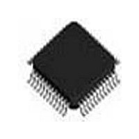
PEB3081FV14XP Lantiq, PEB3081FV14XP Datasheet - Page 50

PEB3081FV14XP
Manufacturer Part Number
PEB3081FV14XP
Description
Manufacturer
Lantiq
Datasheet
1.PEB3081FV14XP.pdf
(198 pages)
Specifications of PEB3081FV14XP
Number Of Line Interfaces
1
Control Interface
HDLC
Lead Free Status / Rohs Status
Compliant
- Current page: 50 of 198
- Download datasheet (3Mb)
Preliminary
Protection Circuit for Transmitter
Figure 24
Figure 24
The external resistors (R = 5 .... 10
to the pulse mask on the one hand and in order to meet the output impedance of
minimum 20
hand.
Two mutually reversed diode paths protect the device against positive or negative
overvoltages on both lines.
An ideal protection circuit should limit the voltage at the SX pins from – 0.4 V to V
+ 0.4 V. With the circuit in
V
becoming active if the 96 kHz test signal is applied while no supply voltage is present.
Data Sheet
DD
+ 0.7 V. The resulting forward voltage of 1.4 V will prevent the protection circuit from
illustrates the secondary protection circuit recommended for the transmitter.
SX1
SX2
External Circuitry for Transmitter
(transmission of a binary zero according to ITU-T I.430) on the other
Figure 24
R
R
) are required in order to adjust the output voltage
the pin voltage range is increased from – 1.4 V to
50
Vdd
Description of Functional Blocks
1:1
3081_23
S Bus
PEB 3081
PEF 3081
2000-09-27
DD
Related parts for PEB3081FV14XP
Image
Part Number
Description
Manufacturer
Datasheet
Request
R

Part Number:
Description:
Manufacturer:
Lantiq
Datasheet:

Part Number:
Description:
Manufacturer:
Lantiq
Datasheet:

Part Number:
Description:
Manufacturer:
Lantiq
Datasheet:


