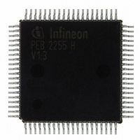
PEB2255H-V13 Infineon Technologies, PEB2255H-V13 Datasheet - Page 116

PEB2255H-V13
Manufacturer Part Number
PEB2255H-V13
Description
IC INTERFACE LINE 80-MQFP
Manufacturer
Infineon Technologies
Datasheet
1.PEB2255H-V13.pdf
(374 pages)
Specifications of PEB2255H-V13
Applications
*
Interface
*
Voltage - Supply
*
Package / Case
80-SQFP
Mounting Type
Surface Mount
Lead Free Status / RoHS Status
Lead free / RoHS Compliant
Other names
PEB2255H-V13
PEB2255H-V13IN
PEB2255H-V13IN
Available stocks
Company
Part Number
Manufacturer
Quantity
Price
Company:
Part Number:
PEB2255H-V13
Manufacturer:
Infineon Technologies
Quantity:
10 000
- Current page: 116 of 374
- Download datasheet (6Mb)
• a receive slip occurred
5.1.12.3 CAS Bit-robbing (T1/J1, µP access mode)
The signaling information is carried in the LSB of every sixth frame for each time slot.
The signaling controller samples the bit stream on the receive line side. Receive
signaling data is stored in the registers RS1-12.
To relieve the µP load from always reading the complete RS1-12 buffer every 3 ms the
FALC
multiframe to the next.
5.1.12.4 Bit Oriented Messages in ESF-DL Channel (T1/J1)
The FALC
T1.403 specification or according to AT&T TR54016. The HDLC- and Bit Oriented
Message (BOM)-Receiver may be switched ON/OFF independently. If the FALC
used for HDLC formats only, the BOM receiver has to be switched off. If HDLC- and
BOM-receiver has been switched on (MODE.HRAC/BRAC), an automatic switching
between HDLC and BOM mode is enabled. If eight or more consecutive ones are
detected, the BOM mode is entered. Upon detection of a flag in the data stream, the
FALC
assumed (the left most bit is received first): 111111110xxxxxx0
Two different BOM reception modes can be programmed (CCR1.BRM).
5.1.12.5 Data Link Access in F72 Format (T1/J1)
The DL-channel protocol is supported as follows:
- access is done on a multiframe basis via registers RDL1-3,
- the DL bit information from frame 26 to 72 is stored in the Receive FIFO of the signaling
controller.
5.2
The interface to the receive system highway is realized by two data buses, one for the
data RDO and one for the signaling data RSIG. The receive highway is clocked via pin
SCLKR, while the interface to the transmit system highway is independently clocked via
pin SCLKX. The frequency of these working clocks and the data rate for the receive and
transmit system interface is programmable by SIC1.SRSC and SIC1.SXSC. Transmit
and receive clock frequencies have to be the same. Selectable system clock and data
rates and their valid combinations are shown in the table below.
Data Sheet
®
®
-LH notifies the µP via interrupt ISR0.RSC only when signaling changes from one
-LH switches back to HDLC-mode. In BOM-mode, the following byte format is
®
System Interface in T1/J1 Mode
-LH supports the DL-channel protocol for ESF format according to ANSI
116
Functional Description T1/J1
FALC-LH V1.3
PEB 2255
2000-07
®
-LH is
Related parts for PEB2255H-V13
Image
Part Number
Description
Manufacturer
Datasheet
Request
R

Part Number:
Description:
E1/t1/j1 Framer And Line Interface Component For Long And Short Haul Applications
Manufacturer:
Infineon Technologies Corporation
Datasheet:

Part Number:
Description:
Manufacturer:
Infineon Technologies AG
Datasheet:

Part Number:
Description:
Manufacturer:
Infineon Technologies AG
Datasheet:

Part Number:
Description:
Manufacturer:
Infineon Technologies AG
Datasheet:

Part Number:
Description:
Manufacturer:
Infineon Technologies AG
Datasheet:

Part Number:
Description:
Manufacturer:
Infineon Technologies AG
Datasheet:

Part Number:
Description:
Manufacturer:
Infineon Technologies AG
Datasheet:

Part Number:
Description:
Manufacturer:
Infineon Technologies AG
Datasheet:

Part Number:
Description:
16-bit microcontroller with 2x2 KByte RAM
Manufacturer:
Infineon Technologies AG
Datasheet:

Part Number:
Description:
NPN silicon RF transistor
Manufacturer:
Infineon Technologies AG
Datasheet:

Part Number:
Description:
NPN silicon RF transistor
Manufacturer:
Infineon Technologies AG
Datasheet:

Part Number:
Description:
NPN silicon RF transistor
Manufacturer:
Infineon Technologies AG
Datasheet:

Part Number:
Description:
NPN silicon RF transistor
Manufacturer:
Infineon Technologies AG
Datasheet:

Part Number:
Description:
Si-MMIC-amplifier in SIEGET 25-technologie
Manufacturer:
Infineon Technologies AG
Datasheet:

Part Number:
Description:
IGBT Power Module
Manufacturer:
Infineon Technologies AG
Datasheet:


