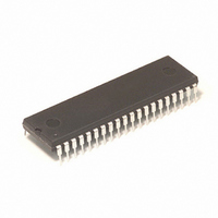
MC908GP32CPE Freescale Semiconductor, MC908GP32CPE Datasheet - Page 159

MC908GP32CPE
Manufacturer Part Number
MC908GP32CPE
Description
IC MCU 8MHZ 32K FLASH 40-DIP
Manufacturer
Freescale Semiconductor
Series
HC08r
Datasheet
1.MC908GP32CFBE.pdf
(266 pages)
Specifications of MC908GP32CPE
Core Processor
HC08
Core Size
8-Bit
Speed
8MHz
Connectivity
SCI, SPI
Peripherals
LVD, POR, PWM
Number Of I /o
33
Program Memory Size
32KB (32K x 8)
Program Memory Type
FLASH
Ram Size
512 x 8
Voltage - Supply (vcc/vdd)
2.7 V ~ 5.5 V
Data Converters
A/D 8x8b
Oscillator Type
Internal
Operating Temperature
-40°C ~ 85°C
Package / Case
40-DIP (0.600", 15.24mm)
Processor Series
HC08GP
Core
HC08
Data Bus Width
8 bit
Data Ram Size
512 B
Interface Type
SCI, SPI
Maximum Clock Frequency
8 MHz
Number Of Programmable I/os
33
Number Of Timers
4
Maximum Operating Temperature
+ 85 C
Mounting Style
Through Hole
Development Tools By Supplier
FSICEBASE, DEMO908GZ60E, M68CBL05CE, M68EML08GPGTE
Minimum Operating Temperature
- 40 C
On-chip Adc
8 bit, 8 Channel
Lead Free Status / RoHS Status
Lead free / RoHS Compliant
Eeprom Size
-
Lead Free Status / Rohs Status
Details
Available stocks
Company
Part Number
Manufacturer
Quantity
Price
Company:
Part Number:
MC908GP32CPE
Manufacturer:
NXP
Quantity:
9 282
Part Number:
MC908GP32CPE
Manufacturer:
FREESCALE
Quantity:
20 000
- Current page: 159 of 266
- Download datasheet (3Mb)
14.2 SIM Bus Clock Control and Generation
The bus clock generator provides system clock signals for the CPU and peripherals on the MCU. The
system clocks are generated from an incoming clock, CGMOUT, as shown in
come from either an external oscillator or from the on-chip PLL. (See
(CGM).)
Freescale Semiconductor
Addr.
$FE03
$FE04
$FE05
$FE06
OSCSTOPENB
CONFIG
FROM
Interrupt Status Register 1
Interrupt Status Register 2
Interrupt Status Register 3
OSC2
OSC1
Register Name
SIM Break Flag Control
Register (SBFCR)
PHASE-LOCKED LOOP (PLL)
CGMRCLK
(INT1)
(INT2)
(INT3)
OSCILLATOR (OSC)
Figure 14-2. SIM I/O Register Summary (Continued)
Reset:
Reset:
Reset:
Reset:
Read:
Read:
Read:
Read:
Write:
Write:
Write:
Write:
Figure 14-3. CGM Clock Signals
Bit 7
BCFE
MC68HC908GP32 Data Sheet, Rev. 10
IF14
IF6
R
R
R
0
0
0
0
0
= Unimplemented
IF13
IF5
CGMXCLK
6
R
R
R
R
0
0
0
0
CGMOUT
SIMDIV2
IF12
IF4
5
R
R
R
R
0
0
0
0
IF11
IF3
4
R
R
R
R
R
0
0
0
0
SIM COUNTER
÷ 2
TO TIMTB15A, ADC
Chapter 5 Clock Generator Module
= Reserved
SIM Bus Clock Control and Generation
IF10
IF2
GENERATORS
R
R
R
R
3
0
0
0
0
SIM
BUS CLOCK
Figure
USER MODE
MONITOR MODE
IF1
IF9
R
R
R
R
2
0
0
0
0
14-3. This clock can
IF16
IF8
1
R
R
R
R
0
0
0
0
SIMOSCEN
PTC3
IT12
TO REST
OF CHIP
IT23
TO REST
OF CHIP
Bit 0
IF15
IF7
R
R
R
R
0
0
0
0
159
Related parts for MC908GP32CPE
Image
Part Number
Description
Manufacturer
Datasheet
Request
R
Part Number:
Description:
Manufacturer:
Freescale Semiconductor, Inc
Datasheet:
Part Number:
Description:
Manufacturer:
Freescale Semiconductor, Inc
Datasheet:
Part Number:
Description:
Manufacturer:
Freescale Semiconductor, Inc
Datasheet:
Part Number:
Description:
Manufacturer:
Freescale Semiconductor, Inc
Datasheet:
Part Number:
Description:
Manufacturer:
Freescale Semiconductor, Inc
Datasheet:
Part Number:
Description:
Manufacturer:
Freescale Semiconductor, Inc
Datasheet:
Part Number:
Description:
Manufacturer:
Freescale Semiconductor, Inc
Datasheet:
Part Number:
Description:
Manufacturer:
Freescale Semiconductor, Inc
Datasheet:
Part Number:
Description:
Manufacturer:
Freescale Semiconductor, Inc
Datasheet:
Part Number:
Description:
Manufacturer:
Freescale Semiconductor, Inc
Datasheet:
Part Number:
Description:
Manufacturer:
Freescale Semiconductor, Inc
Datasheet:
Part Number:
Description:
Manufacturer:
Freescale Semiconductor, Inc
Datasheet:
Part Number:
Description:
Manufacturer:
Freescale Semiconductor, Inc
Datasheet:
Part Number:
Description:
Manufacturer:
Freescale Semiconductor, Inc
Datasheet:
Part Number:
Description:
Manufacturer:
Freescale Semiconductor, Inc
Datasheet:


