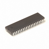
MC908GP32CPE Freescale Semiconductor, MC908GP32CPE Datasheet - Page 182

MC908GP32CPE
Manufacturer Part Number
MC908GP32CPE
Description
IC MCU 8MHZ 32K FLASH 40-DIP
Manufacturer
Freescale Semiconductor
Series
HC08r
Datasheet
1.MC908GP32CFBE.pdf
(266 pages)
Specifications of MC908GP32CPE
Core Processor
HC08
Core Size
8-Bit
Speed
8MHz
Connectivity
SCI, SPI
Peripherals
LVD, POR, PWM
Number Of I /o
33
Program Memory Size
32KB (32K x 8)
Program Memory Type
FLASH
Ram Size
512 x 8
Voltage - Supply (vcc/vdd)
2.7 V ~ 5.5 V
Data Converters
A/D 8x8b
Oscillator Type
Internal
Operating Temperature
-40°C ~ 85°C
Package / Case
40-DIP (0.600", 15.24mm)
Processor Series
HC08GP
Core
HC08
Data Bus Width
8 bit
Data Ram Size
512 B
Interface Type
SCI, SPI
Maximum Clock Frequency
8 MHz
Number Of Programmable I/os
33
Number Of Timers
4
Maximum Operating Temperature
+ 85 C
Mounting Style
Through Hole
Development Tools By Supplier
FSICEBASE, DEMO908GZ60E, M68CBL05CE, M68EML08GPGTE
Minimum Operating Temperature
- 40 C
On-chip Adc
8 bit, 8 Channel
Lead Free Status / RoHS Status
Lead free / RoHS Compliant
Eeprom Size
-
Lead Free Status / Rohs Status
Details
Available stocks
Company
Part Number
Manufacturer
Quantity
Price
Company:
Part Number:
MC908GP32CPE
Manufacturer:
NXP
Quantity:
9 282
Part Number:
MC908GP32CPE
Manufacturer:
FREESCALE
Quantity:
20 000
- Current page: 182 of 266
- Download datasheet (3Mb)
Serial Peripheral Interface Module (SPI)
to accept new data. Write to the transmit data register only when the SPTE bit is high.
the timing associated with doing back-to-back transmissions with the SPI (SPSCK has CPHA: CPOL =
1:0).
The transmit data buffer allows back-to-back transmissions without the slave precisely timing its writes
between transmissions as in a system with a single data buffer. Also, if no new data is written to the data
buffer, the last value contained in the shift register is the next data word to be transmitted.
For an idle master or idle slave that has no data loaded into its transmit buffer, the SPTE is set again no
more than two bus cycles after the transmit buffer empties into the shift register. This allows the user to
queue up a 16-bit value to send. For an already active slave, the load of the shift register cannot occur
until the transmission is completed. This implies that a back-to-back write to the transmit data register is
not possible. The SPTE indicates when the next write can occur.
15.7 Error Conditions
The following flags signal SPI error conditions:
182
•
•
Overflow (OVRF) — Failing to read the SPI data register before the next full byte enters the shift
register sets the OVRF bit. The new byte does not transfer to the receive data register, and the
unread byte still can be read. OVRF is in the SPI status and control register.
Mode fault error (MODF) — The MODF bit indicates that the voltage on the slave select pin (SS)
is inconsistent with the mode of the SPI. MODF is in the SPI status and control register.
CPHA:CPOL = 1:0
WRITE TO SPDR
1
2
3
4 FIRST INCOMING BYTE TRANSFERS FROM SHIFT
5
6 CPU READS SPSCR WITH SPRF BIT SET.
READ SPSCR
CPU WRITES BYTE 1 TO SPDR, CLEARING SPTE BIT.
BYTE 1 TRANSFERS FROM TRANSMIT DATA
REGISTER TO SHIFT REGISTER, SETTING SPTE BIT.
CPU WRITES BYTE 2 TO SPDR, QUEUEING BYTE 2
AND CLEARING SPTE BIT.
REGISTER TO RECEIVE DATA REGISTER, SETTING
SPRF BIT.
BYTE 2 TRANSFERS FROM TRANSMIT DATA
REGISTER TO SHIFT REGISTER, SETTING SPTE BIT.
READ SPDR
SPSCK
SPTE
SPRF
MOSI
1
Figure 15-8. SPRF/SPTE CPU Interrupt Timing
MC68HC908GP32 Data Sheet, Rev. 10
MSB BIT
BYTE 1
2
6
BIT
5
3
BIT
4
BIT
3
BIT
2
BIT
1
10
11 CPU READS SPSCR WITH SPRF BIT SET.
12 CPU READS SPDR, CLEARING SPRF BIT.
7 CPU READS SPDR, CLEARING SPRF BIT.
8
9
LSB MSB BIT
5
4
CPU WRITES BYTE 3 TO SPDR, QUEUEING BYTE
3 AND CLEARING SPTE BIT.
SECOND INCOMING BYTE TRANSFERS FROM SHIFT
REGISTER TO RECEIVE DATA REGISTER, SETTING
SPRF BIT.
BYTE 3 TRANSFERS FROM TRANSMIT DATA
REGISTER TO SHIFT REGISTER, SETTING SPTE BIT.
BYTE 2
6
6
7
BIT
5
8
BIT
4
BIT
3
BIT
2
BIT
1
LSB MSB BIT
10
9
BYTE 3
11
Freescale Semiconductor
6
12
Figure 15-8
BIT
5
BIT
4
shows
Related parts for MC908GP32CPE
Image
Part Number
Description
Manufacturer
Datasheet
Request
R
Part Number:
Description:
Manufacturer:
Freescale Semiconductor, Inc
Datasheet:
Part Number:
Description:
Manufacturer:
Freescale Semiconductor, Inc
Datasheet:
Part Number:
Description:
Manufacturer:
Freescale Semiconductor, Inc
Datasheet:
Part Number:
Description:
Manufacturer:
Freescale Semiconductor, Inc
Datasheet:
Part Number:
Description:
Manufacturer:
Freescale Semiconductor, Inc
Datasheet:
Part Number:
Description:
Manufacturer:
Freescale Semiconductor, Inc
Datasheet:
Part Number:
Description:
Manufacturer:
Freescale Semiconductor, Inc
Datasheet:
Part Number:
Description:
Manufacturer:
Freescale Semiconductor, Inc
Datasheet:
Part Number:
Description:
Manufacturer:
Freescale Semiconductor, Inc
Datasheet:
Part Number:
Description:
Manufacturer:
Freescale Semiconductor, Inc
Datasheet:
Part Number:
Description:
Manufacturer:
Freescale Semiconductor, Inc
Datasheet:
Part Number:
Description:
Manufacturer:
Freescale Semiconductor, Inc
Datasheet:
Part Number:
Description:
Manufacturer:
Freescale Semiconductor, Inc
Datasheet:
Part Number:
Description:
Manufacturer:
Freescale Semiconductor, Inc
Datasheet:
Part Number:
Description:
Manufacturer:
Freescale Semiconductor, Inc
Datasheet:


