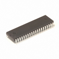
MC908GP32CPE Freescale Semiconductor, MC908GP32CPE Datasheet - Page 180

MC908GP32CPE
Manufacturer Part Number
MC908GP32CPE
Description
IC MCU 8MHZ 32K FLASH 40-DIP
Manufacturer
Freescale Semiconductor
Series
HC08r
Datasheet
1.MC908GP32CFBE.pdf
(266 pages)
Specifications of MC908GP32CPE
Core Processor
HC08
Core Size
8-Bit
Speed
8MHz
Connectivity
SCI, SPI
Peripherals
LVD, POR, PWM
Number Of I /o
33
Program Memory Size
32KB (32K x 8)
Program Memory Type
FLASH
Ram Size
512 x 8
Voltage - Supply (vcc/vdd)
2.7 V ~ 5.5 V
Data Converters
A/D 8x8b
Oscillator Type
Internal
Operating Temperature
-40°C ~ 85°C
Package / Case
40-DIP (0.600", 15.24mm)
Processor Series
HC08GP
Core
HC08
Data Bus Width
8 bit
Data Ram Size
512 B
Interface Type
SCI, SPI
Maximum Clock Frequency
8 MHz
Number Of Programmable I/os
33
Number Of Timers
4
Maximum Operating Temperature
+ 85 C
Mounting Style
Through Hole
Development Tools By Supplier
FSICEBASE, DEMO908GZ60E, M68CBL05CE, M68EML08GPGTE
Minimum Operating Temperature
- 40 C
On-chip Adc
8 bit, 8 Channel
Lead Free Status / RoHS Status
Lead free / RoHS Compliant
Eeprom Size
-
Lead Free Status / Rohs Status
Details
Available stocks
Company
Part Number
Manufacturer
Quantity
Price
Company:
Part Number:
MC908GP32CPE
Manufacturer:
NXP
Quantity:
9 282
Part Number:
MC908GP32CPE
Manufacturer:
FREESCALE
Quantity:
20 000
- Current page: 180 of 266
- Download datasheet (3Mb)
Serial Peripheral Interface Module (SPI)
15.5.3 Transmission Format When CPHA = 1
Figure 15-6
replacement for data sheet parametric information. Two waveforms are shown for SPSCK: one for
CPOL = 0 and another for CPOL = 1. The diagram may be interpreted as a master or slave timing
diagram since the serial clock (SPSCK), master in/slave out (MISO), and master out/slave in (MOSI) pins
are directly connected between the master and the slave. The MISO signal is the output from the slave,
and the MOSI signal is the output from the master. The SS line is the slave select input to the slave. The
slave SPI drives its MISO output only when its slave select input (SS) is at logic 0, so that only the selected
slave drives to the master. The SS pin of the master is not shown but is assumed to be inactive. The SS
pin of the master must be high or must be reconfigured as general-purpose I/O not affecting the SPI. (See
15.7.2 Mode Fault
edge. Therefore, the slave uses the first SPSCK edge as a start transmission signal. The SS pin can
remain low between transmissions. This format may be preferable in systems having only one master and
only one slave driving the MISO data line.
When CPHA = 1 for a slave, the first edge of the SPSCK indicates the beginning of the transmission. This
causes the SPI to leave its idle state and begin driving the MISO pin with the MSB of its data. Once the
transmission begins, no new data is allowed into the shift register from the transmit data register.
Therefore, the SPI data register of the slave must be loaded with transmit data before the first edge of
SPSCK. Any data written after the first edge is stored in the transmit data register and transferred to the
shift register after the current transmission.
15.5.4 Transmission Initiation Latency
When the SPI is configured as a master (SPMSTR = 1), writing to the SPDR starts a transmission. CPHA
has no effect on the delay to the start of the transmission, but it does affect the initial state of the SPSCK
signal. When CPHA = 0, the SPSCK signal remains inactive for the first half of the first SPSCK cycle.
When CPHA = 1, the first SPSCK cycle begins with an edge on the SPSCK line from its inactive to its
active level. The SPI clock rate (selected by SPR1:SPR0) affects the delay from the write to SPDR and
the start of the SPI transmission. (See
derivative of the internal MCU clock. To conserve power, it is enabled only when both the SPE and
SPMSTR bits are set. SPSCK edges occur halfway through the low time of the internal MCU clock. Since
the SPI clock is free-running, it is uncertain where the write to the SPDR occurs relative to the slower
180
CAPTURE STROBE
shows an SPI transmission in which CPHA is logic 1. The figure should not be used as a
FOR REFERENCE
SPSCK; CPOL = 0
SPSCK; CPOL =1
SPSCK CYCLE #
FROM MASTER
SS; TO SLAVE
FROM SLAVE
Error.) When CPHA = 1, the master begins driving its MOSI pin on the first SPSCK
MOSI
MISO
Figure 15-6. Transmission Format (CPHA = 1)
MSB
MSB
MC68HC908GP32 Data Sheet, Rev. 10
1
Figure
BIT 6
BIT 6
2
15-7.) The internal SPI clock in the master is a free-running
BIT 5
BIT 5
3
BIT 4
BIT 4
4
BIT 3
BIT 3
5
BIT 2
BIT 2
6
BIT 1
BIT 1
7
LSB
8
Freescale Semiconductor
LSB
Related parts for MC908GP32CPE
Image
Part Number
Description
Manufacturer
Datasheet
Request
R
Part Number:
Description:
Manufacturer:
Freescale Semiconductor, Inc
Datasheet:
Part Number:
Description:
Manufacturer:
Freescale Semiconductor, Inc
Datasheet:
Part Number:
Description:
Manufacturer:
Freescale Semiconductor, Inc
Datasheet:
Part Number:
Description:
Manufacturer:
Freescale Semiconductor, Inc
Datasheet:
Part Number:
Description:
Manufacturer:
Freescale Semiconductor, Inc
Datasheet:
Part Number:
Description:
Manufacturer:
Freescale Semiconductor, Inc
Datasheet:
Part Number:
Description:
Manufacturer:
Freescale Semiconductor, Inc
Datasheet:
Part Number:
Description:
Manufacturer:
Freescale Semiconductor, Inc
Datasheet:
Part Number:
Description:
Manufacturer:
Freescale Semiconductor, Inc
Datasheet:
Part Number:
Description:
Manufacturer:
Freescale Semiconductor, Inc
Datasheet:
Part Number:
Description:
Manufacturer:
Freescale Semiconductor, Inc
Datasheet:
Part Number:
Description:
Manufacturer:
Freescale Semiconductor, Inc
Datasheet:
Part Number:
Description:
Manufacturer:
Freescale Semiconductor, Inc
Datasheet:
Part Number:
Description:
Manufacturer:
Freescale Semiconductor, Inc
Datasheet:
Part Number:
Description:
Manufacturer:
Freescale Semiconductor, Inc
Datasheet:


