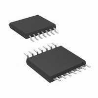
AT89LP214-20XU Atmel, AT89LP214-20XU Datasheet - Page 11

AT89LP214-20XU
Manufacturer Part Number
AT89LP214-20XU
Description
MCU 8051 2K FLASH 20MHZ 14-TSSOP
Manufacturer
Atmel
Series
89LPr
Datasheet
1.AT89LP213-20PU.pdf
(98 pages)
Specifications of AT89LP214-20XU
Core Processor
8051
Core Size
8-Bit
Speed
20MHz
Connectivity
SPI, UART/USART
Peripherals
Brown-out Detect/Reset, POR, PWM, WDT
Number Of I /o
12
Program Memory Size
2KB (2K x 8)
Program Memory Type
FLASH
Ram Size
128 x 8
Voltage - Supply (vcc/vdd)
2.4 V ~ 5.5 V
Oscillator Type
Internal
Operating Temperature
-40°C ~ 85°C
Package / Case
14-TSSOP
Package
14TSSOP
Device Core
8051
Family Name
AT89
Maximum Speed
20 MHz
Operating Supply Voltage
2.5|3.3|5 V
Data Bus Width
8 Bit
Number Of Programmable I/os
12
Interface Type
SPI/UART
Number Of Timers
2
Core
8051
Processor Series
AT89x
Maximum Clock Frequency
20 MHz
Data Ram Size
128 B
Mounting Style
SMD/SMT
Height
1.05 mm
Length
5.1 mm
Maximum Operating Temperature
+ 85 C
Minimum Operating Temperature
- 40 C
Supply Voltage (max)
5.5 V
Supply Voltage (min)
2.4 V
Width
4.5 mm
Lead Free Status / RoHS Status
Lead free / RoHS Compliant
Eeprom Size
-
Data Converters
-
Lead Free Status / Rohs Status
Details
8.1
8.1.1
8.1.2
3538E–MICRO–11/10
Restrictions on Certain Instructions
Branching Instructions
MOVX-related Instructions, Data Memory
Figure 8-3.
The AT89LP213/214 is an economical and cost-effective member of Atmel's growing family of
microcontrollers. It contains 2K bytes of Flash program memory. It is fully compatible with the
MCS-51 architecture, and can be programmed using the MCS-51 instruction set. However,
there are a few considerations one must keep in mind when utilizing certain instructions to pro-
gram this device. All the instructions related to jumping or branching should be restricted such
that the destination address falls within the physical program memory space of the device, which
is 2K for the AT89LP213/214. This should be the responsibility of the software programmer. For
example, LJMP 7E0H would be a valid instruction, whereas LJMP 900H would not.
The LCALL, LJMP, ACALL, AJMP, SJMP, and JMP @A+DPTR unconditional branching instruc-
tions will execute correctly as long as the programmer keeps in mind that the destination
branching address must fall within the physical boundaries of the program memory size (loca-
tions 000H to 7FFH for the AT89LP213/214). Violating the physical space limits may cause
unknown program behavior. With the CJNE [...], DJNZ [...], JB, JNB, JC, JNC, JBC, JZ, and JNZ
conditional branching instructions, the same previous rule applies. Again, violating the memory
boundaries may cause erratic execution. For applications involving interrupts the normal inter-
rupt service routine address locations of the 8051 family architecture have been preserved.
The AT89LP213/214 contains 128 bytes of internal data memory. RAM accesses to addresses
above 7FH will return invalid data. Furthermore, the stack depth is limited to 128 bytes, the
amount of available RAM. The Stack Pointer should not be allowed to point to locations above
7FH. External DATA memory access is not supported in this device, nor is external PROGRAM
memory execution. Therefore, no MOVX [...] instructions should be included in the program.
A typical 8051 assembler will still assemble instructions, even if they are written in violation of
the restrictions mentioned above. It is the responsibility of the user to know the physical features
and limitations of the device being used and to adjust the instructions used accordingly.
Fetch Immediate Operand
ALU Operation Execute
Fetch Next Instruction
Total Execution Time
Result Write Back
Two-cycle ALU Operation (Example: ADD A,
System Clock
T
1
#data
T
2
)
AT89LP213/214
T
3
11


