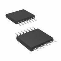
AT89LP214-20XU Atmel, AT89LP214-20XU Datasheet - Page 18

AT89LP214-20XU
Manufacturer Part Number
AT89LP214-20XU
Description
MCU 8051 2K FLASH 20MHZ 14-TSSOP
Manufacturer
Atmel
Series
89LPr
Datasheet
1.AT89LP213-20PU.pdf
(98 pages)
Specifications of AT89LP214-20XU
Core Processor
8051
Core Size
8-Bit
Speed
20MHz
Connectivity
SPI, UART/USART
Peripherals
Brown-out Detect/Reset, POR, PWM, WDT
Number Of I /o
12
Program Memory Size
2KB (2K x 8)
Program Memory Type
FLASH
Ram Size
128 x 8
Voltage - Supply (vcc/vdd)
2.4 V ~ 5.5 V
Oscillator Type
Internal
Operating Temperature
-40°C ~ 85°C
Package / Case
14-TSSOP
Package
14TSSOP
Device Core
8051
Family Name
AT89
Maximum Speed
20 MHz
Operating Supply Voltage
2.5|3.3|5 V
Data Bus Width
8 Bit
Number Of Programmable I/os
12
Interface Type
SPI/UART
Number Of Timers
2
Core
8051
Processor Series
AT89x
Maximum Clock Frequency
20 MHz
Data Ram Size
128 B
Mounting Style
SMD/SMT
Height
1.05 mm
Length
5.1 mm
Maximum Operating Temperature
+ 85 C
Minimum Operating Temperature
- 40 C
Supply Voltage (max)
5.5 V
Supply Voltage (min)
2.4 V
Width
4.5 mm
Lead Free Status / RoHS Status
Lead free / RoHS Compliant
Eeprom Size
-
Data Converters
-
Lead Free Status / Rohs Status
Details
11.2.2
18
AT89LP213/214
Reset Recovery from Power-down
begin. The time-out period is controlled by the Start-up Timer Fuses (see
16). The interrupt pin need not remain low for the entire time-out period.
Figure 11-1. Interrupt Recovery from Power-down (PWDEX = 0)
When PWDEX = “1”, the wake-up period is controlled externally by the interrupt. Again, at the
falling edge on the interrupt pin, power-down is exited and the oscillator is restarted. However,
the internal clock will not propagate until the rising edge of the interrupt pin as shown in
11-2. The interrupt pin should be held low long enough for the selected clock source to stabilize.
After the rising edge on the pin the interrupt service routine will be executed.
Figure 11-2. Interrupt Recovery from Power-down (PWDEX = 1)
The wake-up from Power-down through an external reset is similar to the interrupt with
PWDEX = “0”. At the falling edge of RST, Power-down is exited, the oscillator is restarted, and
an internal timer begins counting as shown in
to propagate to the CPU until after the timer has timed out. The time-out period is controlled by
the Start-up Timer Fuses. (See
a two clock cycle internal reset is generated when the internal clock restarts. Otherwise the
device will remain in reset until RST is brought high.
INTERNAL
INTERNAL
CLOCK
CLOCK
XTAL1
XTAL1
PWD
PWD
INT1
INT1
Table 10-1 on page
Figure
t SUT
16). If RST returns high before the time-out,
11-3. The internal clock will not be allowed
Table 10-1 on page
3538E–MICRO–11/10
Figure


