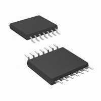
AT89LP214-20XU Atmel, AT89LP214-20XU Datasheet - Page 73

AT89LP214-20XU
Manufacturer Part Number
AT89LP214-20XU
Description
MCU 8051 2K FLASH 20MHZ 14-TSSOP
Manufacturer
Atmel
Series
89LPr
Datasheet
1.AT89LP213-20PU.pdf
(98 pages)
Specifications of AT89LP214-20XU
Core Processor
8051
Core Size
8-Bit
Speed
20MHz
Connectivity
SPI, UART/USART
Peripherals
Brown-out Detect/Reset, POR, PWM, WDT
Number Of I /o
12
Program Memory Size
2KB (2K x 8)
Program Memory Type
FLASH
Ram Size
128 x 8
Voltage - Supply (vcc/vdd)
2.4 V ~ 5.5 V
Oscillator Type
Internal
Operating Temperature
-40°C ~ 85°C
Package / Case
14-TSSOP
Package
14TSSOP
Device Core
8051
Family Name
AT89
Maximum Speed
20 MHz
Operating Supply Voltage
2.5|3.3|5 V
Data Bus Width
8 Bit
Number Of Programmable I/os
12
Interface Type
SPI/UART
Number Of Timers
2
Core
8051
Processor Series
AT89x
Maximum Clock Frequency
20 MHz
Data Ram Size
128 B
Mounting Style
SMD/SMT
Height
1.05 mm
Length
5.1 mm
Maximum Operating Temperature
+ 85 C
Minimum Operating Temperature
- 40 C
Supply Voltage (max)
5.5 V
Supply Voltage (min)
2.4 V
Width
4.5 mm
Lead Free Status / RoHS Status
Lead free / RoHS Compliant
Eeprom Size
-
Data Converters
-
Lead Free Status / Rohs Status
Details
23.8
23.8.1
23.8.2
3538E–MICRO–11/10
Programming Interface Timing
Power-up Sequence
Power-down Sequence
This section details general system timing sequences and constraints for entering or exiting In-
System Programming as well as parameters related to the Serial Peripheral Interface during
ISP. The general timing parameters for the following waveform figures are listed in Section
23.8.6 “Timing Parameters” on page
Execute this sequence to enter programming mode immediately after power-up. In the RST pin
is disabled or if the ISP Fuse is disabled, this is the only method to enter programming (see
tion 10.3 “External Reset” on page
Figure 23-5. Serial Programming Power-up Sequence
Execute this sequence to power-down the device after programming.
Figure 23-6. Serial Programming Power-down Sequence
1. Apply power between VCC and GND pins. RST should remain low.
2. Wait at least t
3. Wait at least t
4. Start programming session.
1. Drive SCK low.
2. Wait at least t
3. Tristate MOSI.
4. Wait at least t
5. Wait no more than t
depend on the current settings of the device.
MISO
MOSI
MISO
MOSI
SCK
RST
V
RST
SCK
V
SS
CC
SS
CC
t
SSD
PWRUP
SUT
SSD
SSZ
and then tristate SS and SCK.
for the internal Power-on Reset to complete. The value of t
and bring SS high.
. and drive SS high.
PWRDN
t
PWRUP
and power off VCC.
16).
t
SSZ
76.
HIGH Z
HIGH Z
HIGH Z
HIGH Z
t
POR
+ t
SUT
t
PWRDN
t
ZSS
AT89LP213/214
SUT
will
Sec-
73


