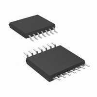
AT89LP214-20XU Atmel, AT89LP214-20XU Datasheet - Page 42

AT89LP214-20XU
Manufacturer Part Number
AT89LP214-20XU
Description
MCU 8051 2K FLASH 20MHZ 14-TSSOP
Manufacturer
Atmel
Series
89LPr
Datasheet
1.AT89LP213-20PU.pdf
(98 pages)
Specifications of AT89LP214-20XU
Core Processor
8051
Core Size
8-Bit
Speed
20MHz
Connectivity
SPI, UART/USART
Peripherals
Brown-out Detect/Reset, POR, PWM, WDT
Number Of I /o
12
Program Memory Size
2KB (2K x 8)
Program Memory Type
FLASH
Ram Size
128 x 8
Voltage - Supply (vcc/vdd)
2.4 V ~ 5.5 V
Oscillator Type
Internal
Operating Temperature
-40°C ~ 85°C
Package / Case
14-TSSOP
Package
14TSSOP
Device Core
8051
Family Name
AT89
Maximum Speed
20 MHz
Operating Supply Voltage
2.5|3.3|5 V
Data Bus Width
8 Bit
Number Of Programmable I/os
12
Interface Type
SPI/UART
Number Of Timers
2
Core
8051
Processor Series
AT89x
Maximum Clock Frequency
20 MHz
Data Ram Size
128 B
Mounting Style
SMD/SMT
Height
1.05 mm
Length
5.1 mm
Maximum Operating Temperature
+ 85 C
Minimum Operating Temperature
- 40 C
Supply Voltage (max)
5.5 V
Supply Voltage (min)
2.4 V
Width
4.5 mm
Lead Free Status / RoHS Status
Lead free / RoHS Compliant
Eeprom Size
-
Data Converters
-
Lead Free Status / Rohs Status
Details
17.3
More About Mode 0
Serial data enters and exits through RXD. TXD outputs the shift clock. Eight data bits are trans-
mitted/received, with the LSB first. The baud rate is fixed at 1/2 the oscillator frequency.
Figure
17-1 on page 43
shows a simplified functional diagram of the serial port in Mode 0 and associ-
ated timing.
Transmission is initiated by any instruction that uses SBUF as a destination register. The “write
to SBUF” signal also loads a “1” into the 9th position of the transmit shift register and tells the TX
Control Block to begin a transmission. The internal timing is such that one full machine cycle will
elapse between “write to SBUF” and activation of SEND.
SEND transfers the output of the shift register to the alternate output function line of P3.0, and
also transfers Shift Clock to the alternate output function line of P3.1. At the falling edge of Shift
Clock the contents of the transmit shift register are shifted one position to the right.
As data bits shift out to the right, “0”s come in from the left. When the MSB of the data byte is at
the output position of the shift register, the “1” that was initially loaded into the 9th position is just
to the left of the MSB, and all positions to the left of that contain “0”s. This condition flags the TX
Control block to do one last shift, then deactivate SEND and set TI.
Reception is initiated by the condition REN = 1 and R1 = 0. At the next clock cycle, the RX Con-
trol unit writes the bits 11111110 to the receive shift register and activates RECEIVE in the next
clock phase.
RECEIVE enables Shift Clock to the alternate output function line of P3.1. At the falling edge of
Shift Clock the contents of the receive shift register are shifted one position to the left. The value
that comes in from the right is the value that was sampled at the P3.0 pin at rising edge of Shift
Clock.
As data bits come in from the right, “1”s shift out to the left. When the “0” that was initially loaded
into the right-most position arrives at the left-most position in the shift register, it flags the RX
Control block to do one last shift and load SBUF. Then RECEIVE is cleared and RI is set.
AT89LP213/214
42
3538E–MICRO–11/10


